
Integration Guide
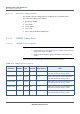

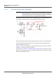
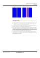
Table Of Contents
- Module Integration Guide
- Preface
- About this Guide
- Introduction
- Manufacturing Process
- Hardware Integration Recommendations
- PCB Layout Rules
- Bring-Up and Testing
- Hardware Test Preparation
- Abbreviations

HARDWARE INTEGRATION RECOMMENDATIONS
RF INTERFACE
MODULE INTEGRATION GUIDE PROPRIETARY 19
SEQUANS Communications
Figure 3-3: Transmission Line Implementation Examples
Figure 3-3 provides examples of both transmission line implementations,
specifically showing:
a) The clearance from the transmission line to adjacent metal on layer 1.
b) The periodic via connections connecting metal-1 layer through to the
reference GND layer for the transmission line.
• Avoid routing of noisy signal tracks adjacent to RF transmission lines to
minimize interference coupling into VZM20Q RF ports.
• The component pads for the SMD terminals of the matching components
used in the 3-component T-type matching circuit are effectively very short
transmission lines. To minimise the RF insertion loss caused by the discon-
tinuity in width differences, the ideal width of the 50 Ohm track should be
as close as possible to the width of the component pads.
• If connectors are used in-line on antenna paths design the PCB interface
tracking and cut-out carefully to these connectors to keep the transmission
line impedance to 50 Ohm.