
Data Sheet
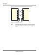
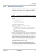
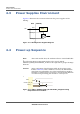
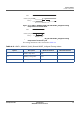
Table Of Contents
- Datasheet
- Preface
- About this Datasheet
- Product Features
- Regulatory Approval
- Physical Characteristics
- 3.1 ECCN and Part Number
- 3.2 Electrical Operating Conditions
- 3.3 Environmental Operating Conditions
- 3.4 Auxiliary ADC Specification
- 3.5 Power Supply Dimensioning
- 3.6 I/O Characteristics
- 3.7 Package Description
- 3.8 Packing Information
- 3.9 Storage Conditions
- 3.10 Mounting Considerations
- 3.11 Component Reliability
- 3.12 RF Performance
- Signals and Pins
- Acronyms

SIGNALS AND PINS
POWER SUPPLIES ENVIRONMENT
37 PROPRIETARY SP150Q DATASHEET
SEQUANS Communications
4.3 Power Supplies Environment
Figure 4-3 illustrates the connections between the power supplies of the
SP150Q.
Figure 4-2: SP150Q Power Supplies Diagram
4.4 Power-up Sequence
Note: After each module boot, the modem will issue +SYSSTART URC.
The following timing requirement applies to the signals VBAT1,
MODULE_PWR_EN and RESET_N. It must be respected for proper SP150Q’s
behavior.
Caution: VBAT1 and VBAT2 should remain stable in the voltage range
listed in Table 3-2; if this condition is not met, the internal OTP
(One-Time Programmable) area of the baseband chip might be
randomly corrupted and it can lead to a non-functional and unre-
coverable state preventing the module to correctly boot.
Figure 4-3: VBAT1, MODULE_PWR_EN and RESET_N Signals Timing
Requirement for Cold Start
WD/
W
sd
sdϭ
sϮͺW
sϭͺW
^WϭϱϬYW
ƚƐϭ
ƚƐ
ŽůĚƐƚĂƌƚ
sdϭ
DKh>ͺWtZͺE
Z^dͺE