
Data Sheet
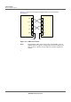

Table Of Contents
- Datasheet
- Preface
- About this Datasheet
- Product Overview
- Physical Characteristics
- Signals and Pins
- Acronyms
- PCB Layout Rules

TRACE CHARACTERISTIC DESIGN
35 PROPRIETARY CB410L DATASHEET
SEQUANS Communications
B.2 Trace Characteristic Design
This section explains some standard design rules when considering different
types of signals involved (digital, power supply, RF).
B.2.1 Digital Traces
1. Careful and logical placement of digital signals are required to ensure sepa-
ration of digital interference between each other and unrelated traces.
2. Consider the flow of ground currents during routing. Make sure that the
grounding surrounding the traces (from source to load) remains contin-
uous, with no cut or breaks. This will avoid long convoluted ground return
currents which can create EMI-type problems.
3. Ensure the steps provided in Section Controlled Impedance Traces are
taken into account for digital traces requiring specific impedance.
4. For those with no impedance requirements, be practical with the trace
thickness. Keep them thin to avoid a buildup of capacitance, but make sure
they are suitable to manufacture.
5. If routing traces on alternate layers, avoid paralleling them and keep them
orthogonal. Good practice is to run traces on alternative layer from vertical
to horizontal and so forth. This avoid traces directly coupling.
6. Important recommendation related to SIM connector placement can be
found in Section ***UNRESOLVED***.
B.2.2 Power Supply Traces
1. Size the power supply traces appropriately for low impedance source. Pay
attention to the number of vias used when routing traces across multiple
layers. This is especially true for high current signals such as PA supply
voltage.
2. For each power supply output, the decoupling capacitors ground pad must
be connected to ground return of the power supply source.
3. Make sure that the digital traces remain well away from the power supply
traces.
4. Appropriate dimensioning of the width and length of each supply track
and the number of any interlayer connecting vias is needed to minimize the
resistive losses in each supply track.