
User's Manual
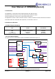
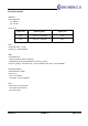

Table Of Contents
- User Manual of SRM200A(Rev1.0)
- 1. Introduction
- 2. Hardware Architecture:
- 2.1 Main Chipset Information
- 2.2 Circuit Block Diagram
- Figure 1-1 SRM200A block diagram and System Interface
- 3. Operational Description
- 3.1 Features
- 3.2 Time base of the RF frequency
- 3.3 Transmission
- 3.4 Receiver
- 3.5 Product Details
- 3.6 Output Power tolerance
- 3.7 SRM200A Category of signal
- 3.8 Simultaneous transmission

3.4 Receiver
-SIGFOX
The Rx path is able to receive sub-1GHz signal and the noise amplifier is built in the inside of the chip, it
amplifies the received signal by the low noise amplifier according to the receiving intensity, and the amplified
signal is converted into the digital signal through the ADC, Packets will be interpreted.
-BLE
The RADIO contains a 2.4 GHz radio receiver and a 2.4 GHz radio transmitter that is compatible with
Nordic's proprietary 1 Mbps radio modes in addition to 1 Mbps Bluetooth® low energy mode.
-WIFI
The 2.4-GHz receiver down-converts the RF signals to quadrature baseband signals and converts them to the
digital domain with 2 high resolution high speed ADCs. To adapt to varying signal channel conditions, RF filters,
automatic gain control (AGC), DC offset cancelation circuits and baseband filters are integrated within ESP8285.
-GPS(GLONASS)
u-blox 8 GNSS chips are single GNSS receivers which can receive and track either GPS or GLONASS signals.
By default the u-blox 8 receivers are configured for GPS, including SBAS and QZSS reception. If power
consumption is a key factor, then QZSS and SBAS should be disabled.
-NFC
The NFCT peripheral (referred to as the 'NFC peripheral' from now on) supports communication signal
interface type A and 106 kbps bit rate from the NFC Forum.
Version 1.0 SEONG JI page 6 of 11