
Data Sheet

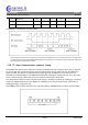


Table Of Contents
- 1. Revision History
- 2. Scope
- 3. Product Information
- 4. Introduction
- 5. Electrical Specifications
- 5-1. Absolute Maximum Ratings
- 5-2. Recommended operating Range
- 5-3. Electrical Characteristics – DC
- 5-4. Electrical Characteristics – RF TX
- 5-5. Electrical Characteristics – RF RX
- 5-6. Electrical Characteristics – RF PLL
- 5-7. Electrical Characteristics – Audio C/CS
- 5-8. AV5100 Rate Converter Characteristics
- 5-9. I2S Communication Interface Timing
- 5-10. I2C Slave Communication Interface Timing
- 6. I/O Connector Pin Description
- 7. Mechanical Specifications
- 7-1. Module dimension
- 7-2. Antenna dimension
- 8. Label Specification
- 9. Certificate Statement

PBA RF Module ATM210
5GHz
Wireless Audio Transceiver
REV: 00
T
Hd
Hold time 25 ns
T
Od
Output delay -25 25 ns
Bit clocks/Word clock 64
I2S protocol is “I2S Justified” as shown below.
*The timing specified for the rise and fall times represents the edge rates on the module itself. The rise and fall times
of the I2S signals are determined by ESD/EMI mitigation components on the modules, as well as external loading, and
will be higher than the specified numbers
5-10. I
2
C Slave Communication Interface Timing
The ATM210 has both I2C slave and master interfaces available with their respective pins S_SCL, S_SDA and
M_SCL, M_SDA. The interfaces operate in I2C fast-mode and can receive and transmit at up to 400 kbit/s.
Bytes are 8 bits long and are transferred with the most significant bit (MSB) first. Each byte has to be
followed by an acknowledge bit. The SWA52 will apply clock-stopping (by holding the clock line S_SCL LOW
to force the master into a wait state) if necessary due to internal high-priority tasks.
The slave/master interface can be used both for writing (e.g. sending commands) or reading (e.g. requesting
status). An additional GPIO pin on the SWA52 (Ex. GPIO24), can be used to notify the I2C master when a
pending message is ready to be sent.
The ATM210 slave interface responds to the 7-bit slave address 1000000 (0x40) as shown in picture below.
12 /20
JUN 10,2019