
User Manual


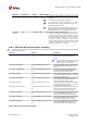


Table Of Contents
- Preface
- Contents
- 1 AT command settings
- 2 General operation
- 3 IPC - Inter Processor Communication
- 4 General
- 4.1 Manufacturer identification +CGMI
- 4.2 Manufacturer identification +GMI
- 4.3 Model identification +CGMM
- 4.4 Model identification +GMM
- 4.5 Firmware version identification +CGMR
- 4.6 Firmware version identification +GMR
- 4.7 Request product serial number identification +CGSN
- 4.8 IMEI identification +GSN
- 4.9 Identification information I
- 4.10 TE character set configuration +CSCS
- 4.11 International mobile subscriber identification +CIMI
- 4.12 Card identification +CCID
- 4.13 Repeat last command A/
- 5 Mobile equipment control and status
- 5.1 Phone activity status +CPAS
- 5.2 Module switch off +CPWROFF
- 5.3 Set module functionality +CFUN
- 5.4 Indicator control +CIND
- 5.5 Configuration of indicator control +UCIND
- 5.6 Mobile termination event reporting +CMER
- 5.7 Clock +CCLK
- 5.8 Set greeting text +CSGT
- 5.9 Automatic time zone update +CTZU
- 5.10 Report mobile termination error +CMEE
- 6 Call control
- 7 Network service
- 7.1 Network parameters definition
- 7.2 Subscriber number +CNUM
- 7.3 Signal quality +CSQ
- 7.4 Extended signal quality +CESQ
- 7.5 Operator selection +COPS
- 7.6 Radio Access Technology (RAT) selection +URAT
- 7.7 Network registration status +CREG
- 7.8 Network selection control +PACSP
- 7.9 Channel and network environment description +UCGED
- 7.10 Edit Verizon wireless APN table +VZWAPNE
- 7.11 Read RSRP values +VZWRSRP
- 7.12 Read RSRQ values +VZWRSRQ
- 7.13 Signalling connection status +CSCON
- 7.14 eDRX setting +CEDRXS
- 7.15 eDRX read dynamic parameters +CEDRXRDP
- 7.16 Set MNO profile +UMNOPROF
- 7.17 Band selection bitmask +UBANDMASK
- 7.18 Device service domain configuration +USVCDOMAIN
- 7.19 CIoT optimization configuration +CCIOTOPT
- 7.20 NB-IoT band scan tuning +UDCONF=77
- 8 Device lock
- 9 Short Messages Service
- 9.1 Introduction
- 9.2 Select message service +CSMS
- 9.3 Preferred message storage +CPMS
- 9.4 Preferred message format +CMGF
- 9.5 Save settings +CSAS
- 9.6 Restore settings +CRES
- 9.7 Show text mode parameters +CSDH
- 9.8 New message indication +CNMI
- 9.9 Read message +CMGR
- 9.10 New message acknowledgement to MT +CNMA
- 9.11 List message +CMGL
- 9.12 Send message +CMGS
- 9.13 Write message to memory +CMGW
- 9.14 Send message from storage +CMSS
- 9.15 Set text mode parameters +CSMP
- 9.16 Delete message +CMGD
- 9.17 Service center address +CSCA
- 9.18 Read concatenated message +UCMGR
- 9.19 List concatenated message +UCMGL
- 9.20 Send concatenated message +UCMGS
- 9.21 Write concatenated message to memory +UCMGW
- 9.22 More messages to send +CMMS
- 9.23 Sending of originating data via the control plane +CSODCP
- 9.24 Terminating data reporting via control plane +CRTDCP
- 10 V24 control and V25ter
- 10.1 Introduction
- 10.2 Circuit 109 behavior &C
- 10.3 Circuit 108/2 behavior &D
- 10.4 DSR override &S
- 10.5 DTE-DCE character framing +ICF
- 10.6 DTE-DCE local flow control +IFC
- 10.7 Set flow control \Q
- 10.8 UART data rate configuration +IPR
- 10.9 Return to on-line data state O
- 10.10 Escape character S2
- 10.11 Command line termination character S3
- 10.12 Response formatting character S4
- 10.13 Command line editing character S5
- 10.14 Pause before blind dialling S6
- 10.15 Connection completion timeout S7
- 10.16 Command dial modifier time S8
- 10.17 Automatic disconnect delay S10
- 10.18 Escape prompt delay (EPD) S12
- 10.19 Command echo E
- 10.20 Result code suppression Q
- 10.21 DCE response format V
- 10.22 Result code selection and call progress monitoring control X
- 10.23 Reset to default configuration Z
- 10.24 Set to factory defined configuration &F
- 10.25 Display current configuration &V
- 11 SIM management
- 12 SIM toolkit
- 13 Packet switched data services
- 13.1 PDP contexts and parameter definition
- 13.2 PPP LCP handshake behaviour
- 13.3 Printing IP address format +CGPIAF
- 13.4 PDP context definition +CGDCONT
- 13.5 Packet switched data configuration +UPSD
- 13.6 GPRS attach or detach +CGATT
- 13.7 PDP context activate or deactivate +CGACT
- 13.8 Enter PPP state/GPRS dial-up D*
- 13.9 Show PDP address +CGPADDR
- 13.10 Packet switched event reporting +CGEREP
- 13.11 GPRS network registration status +CGREG
- 13.12 UE modes of operation for EPS +CEMODE
- 13.13 EPS network registration status +CEREG
- 13.14 Delete non-active PDP contexts +CGDEL
- 13.15 Configure the authentication parameters of a PDP/EPS bearer +UAUTHREQ
- 13.16 PDP context read dynamic parameters +CGCONTRDP
- 13.17 Initial PDP context activation +CIPCA
- 13.18 PDP IP configuration when roaming +UDCONF=75
- 13.19 Disable data when roaming +UDCONF=76
- 14 System features
- 14.1 Firmware installation +UFWINSTALL
- 14.2 Firmware update Over AT (FOAT) +UFWUPD
- 14.3 Antenna detection +UANTR
- 14.4 End user test +UTEST
- 14.5 Internal temperature monitor +UTEMP
- 14.6 Back up the file system +UBKUPDATA
- 14.7 Cancel FOTA download +UFOTA
- 14.8 Sets FOTA status URCs +UFOTASTAT
- 14.9 uFOTA configuration +UFOTACONF
- 14.10 Last gasp configuration +ULGASP
- 14.11 RING line configuration +URINGCFG
- 15 Power management
- 16 GPIO
- 16.1 Introduction
- 16.1.1 GPIO functions
- 16.1.2 GPIO mapping
- 16.1.3 Network status indication
- 16.1.3.1 No service (no network coverage or not registered)
- 16.1.3.2 Registered home network 2G
- 16.1.3.3 Registered home network 3G
- 16.1.3.4 Registered home network NB1 / NB2
- 16.1.3.5 Registered roaming 2G
- 16.1.3.6 Registered roaming 3G
- 16.1.3.7 Registered roaming NB1 / NB2
- 16.1.3.8 Data transmission
- 16.1.3.9 Data transmission roaming
- 16.1.4 Module status indication
- 16.1.5 Module operating mode indication
- 16.2 GPIO select configuration command +UGPIOC
- 16.3 GPIO read command +UGPIOR
- 16.4 GPIO set command +UGPIOW
- 16.1 Introduction
- 17 File System
- 18 DNS
- 19 Internet protocol transport layer
- 19.1 Introduction
- 19.2 IPv4/IPv6 addressing
- 19.3 Create Socket +USOCR
- 19.4 SSL/TLS/DTLS mode configuration on TCP/UDP socket +USOSEC
- 19.5 Set socket option +USOSO
- 19.6 Get Socket Option +USOGO
- 19.7 Close Socket +USOCL
- 19.8 Get Socket Error +USOER
- 19.9 Connect Socket +USOCO
- 19.10 Write socket data +USOWR
- 19.11 SendTo command (UDP only) +USOST
- 19.12 Read Socket Data +USORD
- 19.13 Receive From command (UDP only) +USORF
- 19.14 Set Listening Socket +USOLI
- 19.15 HEX mode configuration +UDCONF=1
- 19.16 Set socket in Direct Link mode +USODL
- 19.17 UDP Direct Link Packet Size configuration +UDCONF=2
- 19.18 UDP Direct Link Sending timer configuration +UDCONF=3
- 19.19 Timer Trigger configuration for Direct Link +UDCONF=5
- 19.20 Data Length Trigger configuration for Direct Link +UDCONF=6
- 19.21 Character trigger configuration for Direct Link +UDCONF=7
- 19.22 Direct Link disconnect DSR line handling +UDCONF=10
- 19.23 Socket control +USOCTL
- 19.24 Configure Dormant Close Socket Behavior +USOCLCFG
- 20 Device and data security
- 20.1 Introduction
- 20.2 Device security
- 20.3 Data security
- 20.3.1 Introduction
- 20.3.1.1 SSL/TLS/DTLS
- 20.3.1.2 SARA-R410M-63B / SARA-R410M-73B / SARA-R410M-83B Local encryption and decryption
- 20.3.1.3 SARA-R410M-63B / SARA-R410M-73B / SARA-R410M-83B Pre-Shared Keys (PSK) provisioning
- 20.3.1.4 SARA-R410M-63B / SARA-R410M-73B / SARA-R410M-83B End-to-end data encryption and decryption
- 20.3.2 SSL/TLS certificates and private keys manager +USECMNG
- 20.3.3 SSL/TLS/DTLS security layer profile manager +USECPRF
- 20.3.4 AT+USECMNG command example
- 20.3.5 Notes
- 20.3.6 Local encryption from AT interface +USECDATAENC
- 20.3.7 Local decryption from AT interface +USECDATADEC
- 20.3.8 Local encryption from a file +USECFILEENC
- 20.3.9 Local decryption from a file +USECFILEDEC
- 20.3.10 Pre-Shared Key (PSK) generation +USECPSK
- 20.3.11 End to end encryption from AT interface +USECE2EDATAENC
- 20.3.12 End to end encryption from a file +USECE2EFILEENC
- 20.3.1 Introduction
- 21 FTP
- 22 HTTP
- 23 Positioning
- 23.1 NMEA
- 23.2 AssistNow services
- 23.3 GNSS
- 23.3.1 GNSS power management +UGPS
- 23.3.2 Assisted GNSS unsolicited indication +UGIND
- 23.3.3 GNSS profile configuration +UGPRF
- 23.3.4 Aiding server configuration +UGSRV
- 23.3.5 GNSS aiding request command +UGAOS
- 23.3.6 Send of UBX string +UGUBX
- 23.3.7 GNSS indications timer +UGTMR
- 23.3.8 Get GNSS time and date +UGZDA
- 23.3.9 Get GNSS fix data +UGGGA
- 23.3.10 Get geographic position +UGGLL
- 23.3.11 Get number of GNSS satellites in view +UGGSV
- 23.3.12 Get recommended minimum GNSS data +UGRMC
- 23.3.13 Get course over ground and ground speed +UGVTG
- 23.3.14 Get satellite information +UGGSA
- 23.4 CellLocate and hybrid positioning
- 24 I2C
- 25 MQTT
- 26 Lightweight M2M
- 26.1 LwM2M Objects management
- 26.1.1 Introduction
- 26.1.2 Load LwM2M object definition +ULWM2MADD
- 26.1.3 Remove LwM2M object definition +ULWM2MREMOVE
- 26.1.4 List available LwM2M objects +ULWM2MLIST
- 26.1.5 Create new instance of LwM2M object +ULWM2MCREATE
- 26.1.6 Delete instance of LwM2M object +ULWM2MDELETE
- 26.1.7 Write to LwM2M object +ULWM2MWRITE
- 26.1.8 Read from LwM2M object +ULWM2MREAD
- 26.2 LwM2M connectivity
- 26.2.1 SARA-R4 Command line and information text response maximum length for LwM2M connectivity features
- 26.2.2 LwM2M URCs configuration +ULWM2MSTAT
- 26.2.2.1 SARA-R410M-02B / SARA-R410M-52B / SARA-R410M-63B / SARA-R410M-73B / SARA-R410M-83B / SARA-R412M Description
- 26.2.2.2 SARA-R410M-02B / SARA-R410M-52B / SARA-R410M-63B / SARA-R410M-73B / SARA-R410M-83B / SARA-R412M Syntax
- 26.2.2.3 SARA-R410M-02B / SARA-R410M-52B / SARA-R410M-63B / SARA-R410M-73B / SARA-R410M-83B / SARA-R412M Defined values
- 26.2.2.4 SARA-R404M / SARA-R410M-01B / SARA-R410M-02B / SARA-R410M-52B / SARA-R412M / SARA-N4 Description
- 26.2.2.5 SARA-R404M / SARA-R410M-01B / SARA-R410M-02B / SARA-R410M-52B / SARA-R412M / SARA-N4 Syntax
- 26.2.2.6 SARA-R404M / SARA-R410M-01B / SARA-R410M-02B / SARA-R410M-52B / SARA-R412M / SARA-N4 Defined values
- 26.2.3 Stop LwM2M client +ULWM2M
- 26.2.3.1 SARA-R410M-02B / SARA-R410M-52B / SARA-R410M-63B / SARA-R410M-73B / SARA-R410M-83B / SARA-R412M Description
- 26.2.3.2 SARA-R410M-02B / SARA-R410M-52B / SARA-R410M-63B / SARA-R410M-73B / SARA-R410M-83B / SARA-R412M Syntax
- 26.2.3.3 SARA-R410M-02B / SARA-R410M-52B / SARA-R410M-63B / SARA-R410M-73B / SARA-R410M-83B / SARA-R412M Defined values
- 26.2.3.4 SARA-R404M / SARA-R410M-01B / SARA-R410M-02B / SARA-R410M-52B / SARA-R412M / SARA-N4 Description
- 26.2.3.5 SARA-R404M / SARA-R410M-01B / SARA-R410M-02B / SARA-R410M-52B / SARA-R412M / SARA-N4 Syntax
- 26.2.3.6 SARA-R404M / SARA-R410M-01B / SARA-R410M-02B / SARA-R410M-52B / SARA-R412M / SARA-N4 Defined values
- 26.2.3.7 Notes
- 26.2.4 Initiate LwM2M server registration +ULWM2MREG
- 26.2.5 LwM2M server deregistration +ULWM2MDEREG
- 26.2.6 LwM2M server configuration +ULWM2MCONFIG
- 26.2.7 LwM2M host device information +UHOSTDEV
- 26.2.8 Lightweight M2M pulse configuration +ULWM2MPULSE
- 26.2.9 LwM2M object notification +ULWM2MNOTIFY
- 26.2.10 LwM2M host device information +ODIS
- 26.1 LwM2M Objects management
- A Appendix: Error result codes
- A.1 Mobile termination error result codes +CME ERROR
- A.2 Message service error result codes +CMS ERROR
- A.3 Firmware install final result codes
- A.4 FOAT error result codes
- A.5 Internal TCP/UDP/IP stack class error codes
- A.6 Internet suite error classes
- B Appendix: AT Commands List
- C Appendix: UDP Direct Link workflow
- D Appendix: Glossary
- Related documents
- Revision history
- Contact

SARA-R4 series-AT commands manual
UBX-17003787 - R16
14System features
Page 169 of 401
Command Response Description
AT+UTEST=3,32,7,5 +UTEST: 32,7,5,1,1000
OK
The module will transmit for 1 s interval 1
slot burst sequence at TX channel 32 GSM
900 at PCL 5 using training sequence 5
and normal GMSK modulation.
AT+UTEST=3,65,8,,2,5000 +UTEST: 65,8,5,2,5000
OK
The module will transmit for 5 s interval 1
slot burst sequence at TX channel 65 GSM
900 at PCL 8 (gamma 6, 27 dBm) using
training sequence 5 and normal 8-PSK
modulation.
AT+UTEST=3,660,,,,0 +UTEST: 660,5,5,1,0
OK
The module will transmit continuously 1
slot burst sequence at TX channel 660
DCS 1800 at PCL 5 using training sequence
5 and normal GMSK modulation.
AT+UTEST=3,9612,22,,,2000 +UTEST: 9612,22,5,1,2000
OK
The module will transmit for 2 s interval at
TX channel 9612 band B1 at 22 dBm power
level using WCDMA modulation.
AT+UTEST=3,120399,15,,,3000 +UTEST: 120399,15,5,1,3000
OK
The module transmits for 3 s interval
at TX channel 20399 band FDD 4 at 15
dBm power level using SC-FDMA OFDM
modulation 5 MHz bandwidth.
AT+UTEST=3,123230,-10,,,0 +UTEST: 123230,-10,5,1,0
OK
The module continuously transmits at
TX channel 23230 band FDD 13 at -10
dBm power level using SC-FDMA OFDM
modulation 5 MHz bandwidth.
Table 12: TX mode test command examples
14.4.7Digital pins testing description
Defines the commands to perform some verifications on all the digital pins of the u-blox cellular modules.
These pins can be considered as generic digital input / output pins; it is possible to configure one pin as a digital
output with "high" logic level and then verify the voltage level present. Conversely, it is possible set a pin as
a digital input, externally apply a "high" or "low" logic level and then check if the module is able to correctly
measure the voltage level applied.
After the execution of the AT+UTEST=10,5 command, it is possible to externally apply a voltage level to the
enabled input pins and / or measure the voltage level on the pins configured as digital input.
These commands are intended for production to check the correct digital pins behavior, detect possible
soldering or functional problems and can be executed only in non-signalling mode (otherwise the "+CME
ERROR: operation not allowed" or "+CME ERROR: 3" error result code - depending on the +CMEE AT
command setting - is issued without performing any operations).
Do not exceed the values reported in the Generic Digital Interface section of the module data sheet
when testing a pin as a digital input pin, since stressing the device above the listed ratings may cause a
permanent damage of the module.
The <op_code>, <bit_padding>, <pin_seq> parameters setting is not stored in the NVM.
SARA-R4 / SARA-N4
See the SARA-R4 application development guide [177] and the corresponding module data sheet for the
list of pins available for testing and their levels characteristics and further test command examples.
14.4.8Syntax
Type Syntax Response Example
Digital pins testing generic syntax
Set AT+UTEST=10,<op_code>[,[<bit_
padding>]<pin_seq>]
OK AT+UTEST=10,3,"0000001000000
300"
OK
Original configuration restoring
Set AT+UTEST=10,0 OK AT+UTEST=10,0