
User Manual

7
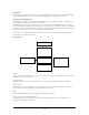
Recommended PCB Layout
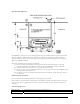
The OEM100 occupies 2.35” by 1.58” and is designed to plug into a PCB mounted, 41 position, Hirose DF9
receptacle (Hirose p/n DF9A-41S-1V(20)). Please refer to Hirose’s documentation for more information
about this connector. There are three mounting holes designed to accommodate 4mm plastic stacking posts
(Richco p/n MDLSP1-04M-01).
There are four distinct areas of the carrier board PCB:
(A) This is reserved for the OEM100’s radio signals, and this area should be kept clear of all metal
components including traces and planes. Note, this zone extended above and below the PCB.
(B) In this area there are no restrictions on component placement or height.
(C) On the top layer, components should be limited to 0.125” in height to fit below the OEM100. On all
other layers there are no restrictions.
(D) On the top layer, the only component should be the Hirose receptacle. On all other layers there are
no restrictions.
Product Labeling Information
Please see important FCC labeling information at the beginning of this manual.
Each module is programmed with a unique address. This address is printed on the barcode label on the back
of the module. In most applications it is helpful to reproduce this label on the outside of the final product
packaging.
Technical Specifications
Radio frequency 902-928MHz Frequency Hopping Spread Spectrum
Radio power +10dBm (10mW) nominal