ESP8266 802.
ESP8266 802.11bgn Smart Device Disclaimer and Copyright Notice Information in this document, including URL references, is subject to change without notice. THIS DOCUMENT IS PROVIDED "AS IS" WITH NO WARRANTIES WHATSOEVER, INCLUDING ANY WARRANTY OF MERCHANTABILITY, NONINFRINGEMENT, FITNESS FOR ANY PARTICULAR PURPOSE, OR ANY WARRANTY OTHERWISE ARISING OUT OF ANY PROPOSAL, SPECIFICATION OR SAMPLE.
ESP8266 802.11bgn Smart Device Table of Contents 1 2 3 4 5 INTRODUCTION TECHNOLOGY OVERVIEW FEATURES APPLICATION DIAGRAM ULTRA LOW POWER TECHNOLOGY 5.1 HIGHEST LEVEL OF INTEGRATION 6 7 ESP8266 APPLICATIONS SPECIFICATIONS 7.1 CURRENT CONSUMPTION 9 10 10 7.2 11 8 4 5 6 7 8 8 RF PERFORMANCE CPU, MEMORY AND INTERFACES 8.1 CPU 12 12 8.2 MEMORY CONTROLLER 12 8.3 AHB AND AHB BLOCKS 12 8.4 INTERFACES 13 8.4.1 Master SI / SPI Control (Optional) 13 8.4.2 General Purpose IO 14 8.4.
ESP8266 802.11bgn Smart Device 1 Introduction Espressif Systems’ Smart Connectivity Platform (ESCP) of high performance wireless SOCs, for mobile platform designers, provides unsurpassed ability to embed Wi-Fi capabilities within other Analog receive RF transmit Analog transmit PLL PMU VCO Crystal 1/2 Digital baseband RF receive Switch RF balun systems, at the lowest cost with the greatest functionality.
ESP8266 802.11bgn Smart Device 2 Technology Overview ESP8266 offers a complete and self-contained Wi-Fi networking solution, allowing it to either host the application or to offload all Wi-Fi networking functions from another application processor. When ESP8266 hosts the application, and when it is the only application processor in the device, it is able to boot up directly from an external flash.
ESP8266 802.11bgn Smart Device 3 Features 802.11 b/g/n protocol Wi-Fi Direct (P2P), soft-AP Integrated TCP/IP protocol stack Integrated TR switch, balun, LNA, power amplifier and matching network Integrated PLL, regulators, and power management units +19.5dBm output power in 802.11b mode Integrated temperature sensor Supports antenna diversity Power down leakage current of < 10uA Integrated low power 32-bit CPU could be used as application processor SDIO 2.
ESP8266 802.
ESP8266 802.11bgn Smart Device 5 Ultra Low Power Technology ESP8266 has been designed for mobile, wearable electronics and Internet of Things applications with the aim of achieving the lowest power consumption with a combination of several proprietary techniques. The power saving architecture operates in 3 modes: active mode, sleep mode and deep sleep mode.
ESP8266 802.
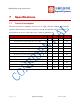
ESP8266 802.11bgn Smart Device 7 Specifications 7.1 Current Consumption The following current consumption is based on 3.3V supply, and 25C ambient, using internal regulators. Measurements are done at antenna port without SAW filter. All the transmitter’s measurements are based on 90% duty cycle, continuous transmit mode. Mode Min Typ Max Unit Transmit 802.11b, CCK 1Mbps, POUT=+19.5dBm 215 mA Transmit 802.11b, CCK 11Mbps, POUT=+18.5dBm 197 mA Transmit 802.
ESP8266 802.11bgn Smart Device 7.2 RF Performance The following are measured under room temperature conditions with 3.3V and 1.1V power supplies. Description Min Input frequency 2412 Input impedance Typical Max Unit 2484 MHz 50 Input reflection -10 dB Output power of PA for 72.2Mbps 14 15 16 dBm Output power of PA for 11b mode 17.5 18.5 19.
ESP8266 802.11bgn Smart Device 8 CPU, Memory and Interfaces 8.1 CPU This chip embeds an ultra low power Micro 32-bit CPU, with 16-bit thumb mode. This CPU can be interfaced using: code RAM/ROM interface (iBus) that goes to the memory controller, that can also be used to access external flash memory, data RAM interface (dBus), that also goes to the memory controller AHB interface, for register access, and JTAG interface for debugging 8.
ESP8266 802.11bgn Smart Device The APB block acts as a decoder. It is meant only for access to programmable registers within ESP8266’s main blocks. Depending on the address, the APB request can go to the radio, SI/SPI, SDIO (host), GPIO, UART, real-time clock (RTC), MAC or digital baseband. 8.4 Interfaces The ESP8266 contains several analog and digital interfaces described in the following sections. 8.4.
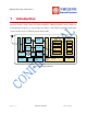
ESP8266 802.11bgn Smart Device SPI_EN2 usually controls an EEPROM to store individual data, such as MIB information, MAC address, and calibration data, or for general use. This pin is active low and should be left open if not used. Figure 2: SPI timing characteristics 8.4.2 General Purpose IO There are up to 16 GPIO pins. They can be assigned to various functions by the firmware.
ESP8266 802.11bgn Smart Device Optional hold functionality can be built into the IO if requested. When the IO is not driven by the internal or external circuitry, the hold functionality can be used to hold the state to the last used state. The hold functionality introduces some positive feedback into the pad. Hence, the external driver that drives the pad must be stronger than the positive feedback. The required drive strength is however small – in the range of 5uA.
ESP8266 802.11bgn Smart Device 9 Firmware & Software Development Kit The application and firmware is executed in on-chip ROM and SRAM, which loads the instructions during wake-up, through the SDIO interface, from the external flash. The firmware implements TCP/IP, the full 802.11 b/g/n/e/i WLAN MAC protocol and Wi-Fi Direct specification.
ESP8266 802.11bgn Smart Device WPA/WPA2 PSK, and WPS driver; Additional 802.11i security features such as pre-authentication, and TSN; Open Interface for various upper layer authentication schemes over EAP such as TLS, PEAP, LEAP, SIM, AKA, or customer specific; 802.11n support (2.4GHz / 5GHz); Supports MIMO 11 and 21, STBC, A-MPDU and A-MSDU aggregation and 0.
ESP8266 802.11bgn Smart Device 10 Power Management The chip can be put into the following states: OFF: CHIP_PD pin is low. The RTC is CHIP_PWD disabled. All registers are cleared. Off DEEP_SLEEP: Only RTC is powered on – the rest of the chip is powered off. ~CHIP_PWD Recovery memory of RTC can keep basic Deep Sleep Wi-Fi connecting information. SLEEP: Only the RTC is operating. The crystal oscillator is disabled.
ESP8266 802.11bgn Smart Device 11 Clock Management 11.1 High Frequency Clock The high frequency clock on ESP8266 is used to drive both the Tx and Rx mixers. This clock is generated from the internal crystal oscillator and an external crystal. The crystal frequency can range from 26MHz to 52MHz. While internal calibration of the crystal oscillator ensures that a wide range of crystals can be used, in general, the quality of the crystal is still a factor to consider, to obtain reasonable phase noise.
ESP8266 802.11bgn Smart Device 11.2 External Reference Requirements For an externally generated clock, the frequency can range from 26MHz to 52MHz can be used. For good performance of the radio, the following characteristics are expected of the clock: Parameter Symbol Min Max Unit Clock amplitude VXO 0.
ESP8266 802.11bgn Smart Device 12 Radio The ESP8266 radio consists of the following main blocks: 2.4GHz receiver 2.4GHz transmitter High speed clock generators and crystal oscillator Real time clock Bias and regulators Power management 12.1 Channel Frequencies The RF transceiver supports the following channels according to the IEEE802.11bgn standards. 12.
ESP8266 802.11bgn Smart Device 12.3 2.4GHz Transmitter The 2.4GHz transmitter upconverts the quadrature baseband signals to 2.4GHz, and drives the antenna with a high powered CMOS power amplifier. The use of digital calibration further improves the linearity of the power amplifier, enabling a state of art performance of delivering +19dBm average power for 802.11b transmission and +16dBm for 802.11n transmission.
ESP8266 802.11bgn Smart Device App.