
Data Sheet

Overview VL53L0X
8/40 DocID029104 Rev 2
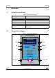
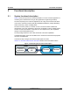
1.4 Application schematic
Figure 3 shows the application schematic of the VL53L0X.
Figure 3. VL53L0X schematic
Note: Capacitors on external supply AVDD should be placed as close as possible to the
AVDDVCSEL and AVSSVCSEL module pins.
Note: External pull-up resistors values can be found in I2C-bus specification. Pull-up are typically
fitted only once per bus, near the host.
Recommended values for pull-up resistors for an AVDD of 2.8V and 400KHz I
2
C clock
would be 1.5k to 2k Ohms.
Note: XSHUT pin must always be driven to avoid leakage current. Pull-up is needed if the host
state is not known.
XSHUT is needed to use HW standby mode (no I
2
C comm).
Note: XSHUT and GPIO1 pull up recommended values are 10k Ohms
Note: GPIO1 to be left unconnected if not used
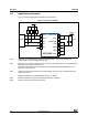
9//;
;6+87
*3,2
6'$
6&/
+267
'1&
$9''9&6(/
$9''
Q) )
$9''
$9669&6(/
*1'
*1'
*1'
*1'
,29''