
Data Sheet

DocID029104 Rev 2 7/40
VL53L0X Overview
37
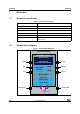
1.3 Device pinout
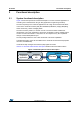
Figure 2 shows the pinout of the VL53L0X (see also Figure 22).
Figure 2. VL53L0X pinout (bottom view)
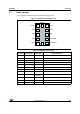
Table 2. VL53L0X pin description
Pin number Signal name Signal type Signal description
1 AVDDVCSEL Supply VCSEL Supply, to be connected to main supply
2 AVSSVCSEL Ground VCSEL Ground, to be connected to main ground
3 GND Ground To be connected to main ground
4 GND2 Ground To be connected to main ground
5 XSHUT Digital input Xshutdown pin, Active LOW
6 GND3 Ground To be connected to main ground
7 GPIO1 Digital output Interrupt output. Open drain output.
8 DNC Digital input Do Not Connect, must be left floating.
9SDA
Digital
input/output
I
2
C serial data
10 SCL Digital input I
2
C serial clock input
11 AVDD Supply Supply, to be connected to main supply
12 GND4 Ground To be connected to main ground
$9''9&6(/
$9669&6(/
*1'
*1'
;6+87
$9''
6&/
6'$
'1&
*3,2
*1'
*1'