
Data Sheet

Control interface VL53L0X
18/40 DocID029104 Rev 2
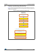
3 Control interface
This section specifies the control interface. The I
2
C interface uses two signals: serial data
line (SDA) and serial clock line (SCL). Each device connected to the bus is using a unique
address and a simple master / slave relationships exists.
Both SDA and SCL lines are connected to a positive supply voltage using pull-up resistors
located on the host. Lines are only actively driven low. A high condition occurs when lines
are floating and the pull-up resistors pull lines up. When no data is transmitted both lines are
high.
Clock signal (SCL) generation is performed by the master device. The master device
initiates data transfer. The I
2
C bus on the VL53L0X has a maximum speed of 400 kbits/s
and uses a device address of 0x52.
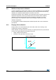
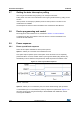
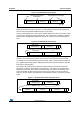
Figure 13. Data transfer protocol
Information is packed in 8-bit packets (bytes) always followed by an acknowledge bit, Ac for
VL53L0X acknowledge and Am for master acknowledge (host bus master). The internal
data is produced by sampling SDA at a rising edge of SCL. The external data must be stable
during the high period of SCL. The exceptions to this are start (S) or stop (P) conditions
when SDA falls or rises respectively, while SCL is high.
A message contains a series of bytes preceded by a start condition and followed by either a
stop or repeated start (another start condition but without a preceding stop condition)
followed by another message. The first byte contains the device address (0x52) and also
specifies the data direction. If the least significant bit is low (that is, 0x52) the message is a
master write to the slave. If the lsb is set (that is, 0x53) then the message is a master read
from the slave.
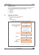
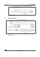
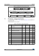
Figure 14. VL53L0X I2C device address: 0x52
All serial interface communications with the camera module must begin with a start
condition. The VL53L0X module acknowledges the receipt of a valid address by driving the
SDA wire low. The state of the read/write bit (lsb of the address byte) is stored and the next
byte of data, sampled from SDA, can be interpreted. During a write sequence the second
byte received provide a 8-bit index which points to one of the internal 8-bit registers.
12
7
8
Ac/Am
Start condition
Stop condition
SDA
SCL
Acknowledge
P
S
3 4 56
Address or data byte
MSB LSB
MSBit
LSBit
0101001R/W