VL53L0X World’s smallest Time-of-Flight ranging and gesture detection sensor Datasheet - production data Applications • User detection for personal computers/ laptops/tablets and IoT (energy saving) • Robotics (obstacle detection) • White goods (hand detection in automatic faucets, soap dispensers etc.) • 1D gesture recognition. Features • Fully integrated miniature module – 940 nm laser VCSEL – VCSEL driver – Ranging sensor with advanced embedded micro controller – 4.4 x 2.4 x 1.
Contents VL53L0X Contents 1 2 Overview . . . . . . . . . . . . . . . . . . . . . . . . . . . . . . . . . . . . . . . . . . . . . . . . . . 6 1.1 Technical specification . . . . . . . . . . . . . . . . . . . . . . . . . . . . . . . . . . . . . . . . 6 1.2 System block diagram . . . . . . . . . . . . . . . . . . . . . . . . . . . . . . . . . . . . . . . . 6 1.3 Device pinout . . . . . . . . . . . . . . . . . . . . . . . . . . . . . . . . . . . . . . . . . . . . . . . 7 1.4 Application schematic . .
VL53L0X 5 Contents 4.3 ESD . . . . . . . . . . . . . . . . . . . . . . . . . . . . . . . . . . . . . . . . . . . . . . . . . . . . . 22 4.4 Current consumption . . . . . . . . . . . . . . . . . . . . . . . . . . . . . . . . . . . . . . . . 23 4.5 Electrical characteristics . . . . . . . . . . . . . . . . . . . . . . . . . . . . . . . . . . . . . . 24 Performance . . . . . . . . . . . . . . . . . . . . . . . . . . . . . . . . . . . . . . . . . . . . . . 25 5.1 Measurement conditions . . . . . . . .
List of tables VL53L0X List of tables Table 1. Table 2. Table 3. Table 4. Table 5. Table 6. Table 7. Table 8. Table 9. Table 10. Table 11. Table 12. Table 13. Table 14. Table 15. Table 16. Table 17. Table 18. Table 19. 4/40 Technical specification . . . . . . . . . . . . . . . . . . . . . . . . . . . . . . . . . . . . . . . . . . . . . . . . . . . . . 6 VL53L0X pin description . . . . . . . . . . . . . . . . . . . . . . . . . . . . . . . . . . . . . . . . . . . . . . . . . . . .
VL53L0X List of figures List of figures Figure 1. Figure 2. Figure 3. Figure 4. Figure 5. Figure 6. Figure 7. Figure 8. Figure 9. Figure 10. Figure 11. Figure 12. Figure 13. Figure 14. Figure 15. Figure 16. Figure 17. Figure 18. Figure 19. Figure 20. Figure 21. Figure 22. Figure 23. Figure 24. Figure 25. Figure 26. Figure 27. Figure 28. VL53L0X block diagram . . . . . . . . . . . . . . . . . . . . . . . . . . . . . . . . . . . . . . . . . . . . . . . . . . . . 6 VL53L0X pinout (bottom view) . . . . . . .
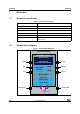
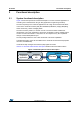
Overview VL53L0X 1 Overview 1.1 Technical specification Table 1. Technical specification Feature 1.2 Detail Package Optical LGA12 Size 4.40 x 2.40 x 1.00 mm Operating voltage 2.6 to 3.5 V Operating temperature: -20 to 70°C Infrared emitter 940 nm I2C Up to 400 kHz (FAST mode) serial bus Address: 0x52 System block diagram Figure 1.
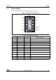
VL53L0X 1.3 Overview Device pinout Figure 2 shows the pinout of the VL53L0X (see also Figure 22). Figure 2. VL53L0X pinout (bottom view) *1' *3,2 '1& ;6+87 *1' 6'$ *1' 6&/ $9669&6(/ $9'' $9''9&6(/ *1' Table 2.
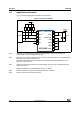
Overview 1.4 VL53L0X Application schematic Figure 3 shows the application schematic of the VL53L0X. Figure 3. VL53L0X schematic ,29'' $9'' +267 ;6+87 $9''9&6(/ *3,2 $9'' 6'$ $9669&6(/ 6&/ *1' '1& *1' *1' 9/ / ; *1' Q) ) Note: Capacitors on external supply AVDD should be placed as close as possible to the AVDDVCSEL and AVSSVCSEL module pins. Note: External pull-up resistors values can be found in I2C-bus specification.
VL53L0X Functional description 2 Functional description 2.1 System functional description Figure 4 shows the system level functional description. The host customer application is controlling the VL53L0X device using an API (Application Programming Interface). The API is exposing to the customer application a set of high level functions that allows control of the VL53L0X Firmware (FW) like initialization/calibration, ranging Start/Stop, choice of accuracy, choice of ranging mode.
Functional description 2.2 VL53L0X Firmware state machine description Figure 5 shows the Firmware state machine. Figure 5.
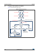
VL53L0X 2.3 Functional description Customer manufacturing calibration flow Figure 6 shows the recommended calibration flow that should be applied at customer level, at factory, once only. This flow takes into account all parameters (cover glass, temperature & voltage) from the application. Figure 6.
Functional description 2.3.1 VL53L0X SPAD and temperature calibration In order to optimize the dynamic of the system, the reference SPADs have to be calibrated. Reference SPAD calibration needs to be done only once during the initial manufacturing calibration, the calibration data should then be stored on the Host. Temperature calibration is the calibration of two parameters (VHV and phase cal) which are temperature dependent. These two parameters are used to set the device sensitivity.
VL53L0X 2.3.3 Functional description Cross-talk calibration Cross-talk is defined as the signal return from the cover glass. The magnitude of the crosstalk depends on the type of glass and air gap. Cross-talk results in a range error which is proportional to the ratio of the cross-talk to the signal return from the target. Measured range Figure 8. Cross-talk compensation cross-talk compensation Actual Range Full offset and cross-talk calibration procedure is described in the VL53L0X API User Manual.
Functional description 2.5 VL53L0X Ranging profiles There are 4 different ranging profiles available via API example code. Customers can create their own ranging profile dependent on their use case performance requirements. For more details please refer to the VL53L0X API User Manual. 2.6 1. Default mode 2. High speed 3. High accuracy 4.
VL53L0X 2.6.1 Functional description Initialization and load calibration data phase Initialization and calibration phase is performed before the first ranging or after a device reset, see Figure 9. The user may then have to repeat the temperature calibration phase in a periodic way, depending on the use case. For more details on the calibration functions please refer to the VL53L0X API User Manual. 2.6.2 Ranging phase The ranging phase consists of a range setup then range measurement.
Functional description 2.7 VL53L0X Getting the data: interrupt or polling User can get the final data using a polling or an interrupt mechanism. Polling mode: user has to check the status of the ongoing measurement by polling an API function. Interrupt mode: An interrupt pin (GPIO1) sends an interrupt to the host when a new measurement is available. The description of these 2 modes is available in the VL53L0X API User Manual. 2.
VL53L0X Functional description Figure 11. Power up and boot sequence with XSHUT not controlled tBOOT is 1.2ms max. 2.10 Ranging sequence Figure 12. Ranging sequence ttiming_budget is a parameter set by the user, using a dedicated API function. Default value is 33ms.
Control interface 3 VL53L0X Control interface This section specifies the control interface. The I2C interface uses two signals: serial data line (SDA) and serial clock line (SCL). Each device connected to the bus is using a unique address and a simple master / slave relationships exists. Both SDA and SCL lines are connected to a positive supply voltage using pull-up resistors located on the host. Lines are only actively driven low.
VL53L0X Control interface Figure 15. VL53L0X data format (write) VL53L0X acknowledges Start S valid address ADDRESS[7:0] Ac INDEX[7:0] Acknowledge from VL53L0X Ac DATA[7:0] 0x52 (write) Ac P Stop As data is received by the slave it is written bit by bit to a serial/parallel register. After each data byte has been received by the slave, an acknowledge is generated, the data is then stored in the internal register addressed by the current index.
Control interface VL53L0X Figure 18. VL53L0X data format (sequential read) 0x52 (write) ADDRESS[7:0] S INDEX[7:0] Ac Ac P 0x53 (read) S ADDRESS[7:0] DATA[7:0] 3.1 DATA[7:0] Ac Am DATA[7:0] Am DATA[7:0] Am DATA[7:0] Am Am P I2C interface - timing characteristics Timing characteristics are shown in Table 3. Please refer to Figure 19 for an explanation of the parameters used. Timings are given for all PVT conditions. Table 3.
VL53L0X Control interface Figure 19. I2C timing characteristics stop start start ... SDA tBUF SCL tLOW tR VIH VIL tHD.STA tF VIH stop ... VIL tHD.STA tHD.DAT tHIGH tSU.DAT tSU.STA tSU.STO All timings are measured from either VIL or VIH. 3.2 I2C interface - reference registers The registers shown in the table below can be used to validate the user I2C interface. Table 4.
Electrical characteristics VL53L0X 4 Electrical characteristics 4.1 Absolute maximum ratings Table 6. Absolute maximum ratings Parameter Min. Typ. Max. Unit AVDD -0.5 - 3.6 V SCL, SDA, XSHUT and GPIO1 -0.5 - 3.6 V Note: Stresses above those listed in Table 6. may cause permanent damage to the device. This is a stress rating only and functional operation of the device at these or any other conditions above those indicated in the operational sections of the specification is not implied.
VL53L0X 4.4 Electrical characteristics Current consumption Table 9. Consumption at ambient temperature(1) Parameter Min. Typ. Max. Unit HW STANDBY 3 5 7 uA SW STANDBY (2V8 mode)(2) 4 6 9 uA Timed ranging Inter measurement 16 uA Active Ranging average consumption (including VCSEL) (3)(4) 19 mA Average power consumption at 10Hz with 33ms ranging sequence 20 mW 1. All current consumption values include silicon process variations.
Electrical characteristics 4.5 VL53L0X Electrical characteristics Table 10. Digital I/O electrical characteristics Symbol Parameter Minimum Typical Maximum Unit Interrupt pin (GPIO1) VIL Low level input voltage - - 0.3 IOVDD V VIH High level input voltage 0.7 IOVDD - - V VOL Low level output voltage (IOUT = 4 mA) - - 0.4 V VOH High level output voltage at (IOUT = 4 mA) IOVDD0.
VL53L0X Performance 5 Performance 5.1 Measurement conditions In all measurement tables in the document, it is considered that the full Field Of View (FOV) is covered. VL53L0X system FOV is 25degrees. Reflectance targets are standard ones (Grey 17% N4.74 and White 88% N9.5 Munsell charts). Unless mentioned, device is controlled through the API using the default settings (refer to VL53L0X API User Manual for API settings description). Figure 20. Typical ranging (default mode) API_RangeValue (mm) vs.
Performance VL53L0X Figure 21. Typical ranging - long range mode API_RangeValue (mm) vs. Actual Target Distance (mm) Reflectance grey17 white88 2200 2000 1800 1600 1400 1200 1000 800 600 400 200 0 5.2 0 200 400 600 800 1000 1200 1400 Actual Target Distance (mm) 1600 1800 2000 2200 2400 Max ranging distance Table 11 presents the ranging specification for VL53L0X bare module, without cover glass, at room temperature (23degreesC) and with nominal voltage (2.8Volts). Table 11.
VL53L0X Performance Note (2): – Indoor: no infrared – Outdoor overcast corresponds to a parasitic noise of 10kcps/SPAD for VL53L0X module. For reference, this corresponds to a 1.2W/m² at 940nm, and is equivalent to 5kLux daylight, while ranging on a grey 17% chart at 40cm Measurement conditions: – Targets reflectance used : Grey (17%), White (88%) – Nominal Voltage (2.
Performance 5.3.2 VL53L0X Range profile examples Table 13 details typical performance for the four example ranging profiles, as per measurement conditions in Section 5.3: Ranging accuracy. Table 13. Range profiles 5.3.3 Range profile Range timing budget Typical performance Typical application Default mode 30 ms 1.2 m, accuracy as per Table 12 Standard High accuracy 200 ms 1.
DocID029104 Rev 2 ) ( ' & /LQHDU 3ODFH 'HFLPDOV 3ODFH 'HFLPDOV 3ODFH 'HFLPDOV $QJXODU GHJUHHV 'LDPHWHU 3RVLWLRQ 6XUIDFH )LQLVK PLFURQV 7ROHUDQFHV XQOHVV RWKHUZLVH VWDWHG )LQLVK 0DWHULDO 3,1 ,QWHUSUHW GUDZLQJ SHU %6 5' $QJOH 3URMHFWLRQ 127(6 ',0(16,216 6+2:1 :,7+ $5( ,163(&7,21 ',0(16,216 68%675$7( :,// $/:$<6 %( ,16,'( 7+( 02'8/( 287/,1( ',
/40 0DWHULDO 'UDZQ $OO GLPHQVLRQV LQ PP 5(9 DocID029104 Rev 2 ) ( ' & /LQHDU 3ODFH 'HFLPDOV 3ODFH 'HFLPDOV 3ODFH 'HFLPDOV $QJXODU GHJUHHV 'LDPHWHU 3RVLWLRQ 6XUIDFH )LQLVK PLFURQV 7ROHUDQFHV XQOHVV RWKHUZLVH VWDWHG (;&/86,21 &21( '$7$ 7+( 7:2 &21(6 6+2:1 21 7+,6 6+((7 5(35(6(17 92/80(6 ,172 :+,&+ 7+( 86(56 (48,30(17 +286,1* 6+28/' 127 (17(5 2) &21(
DocID029104 Rev 2 ) ( ' & % /LQHDU 3ODFH 'HFLPDOV 3ODFH 'HFLPDOV 3ODFH 'HFLPDOV $QJXODU GHJUHHV 'LDPHWHU 3RVLWLRQ 6XUIDFH )LQLVK PLFURQV 7ROHUDQFHV XQOHVV RWKHUZLVH VWDWHG 5 ,1 326 )LQLVK 0DWHULDO 3527(&7,9( /,1(5 ,QWHUSUHW GUDZLQJ SHU %6 5' $QJOH 3URMHFWLRQ '(/,9(5(' &21),*85$7,21 $ '
Laser safety considerations 7 VL53L0X Laser safety considerations The VL53L0X contains a laser emitter and corresponding drive circuitry. The laser output is designed to remain within Class 1 laser safety limits under all reasonably foreseeable conditions including single faults in compliance with IEC 60825-1:2014 (third edition).
VL53L0X Packaging and labeling 8 Packaging and labeling 8.1 Product marking A 2-line product marking is applied on the backside of the module (i.e. on the substrate). The first line is the silicon product code, and the second line, the internal tracking code. Figure 26. Example of marking 8.2 Inner box labeling The labeling follows the ST standard packing acceptance specification. The following information will be on the inner box label: 8.
Packaging and labeling 8.3.1 VL53L0X Tape outline drawings Figure 27. Tape outline drawing Pin 1 8.4 Pb-free solder reflow process Figure 28 and Table 15 shows the recommended and maximum values for the solder profile. Customers will have to tune the reflow profile depending on the PCB, solder paste and material used. We expect customers to follow the “recommended” reflow profile, which is specifically tuned for VL53L0X package.
VL53L0X Packaging and labeling Table 15.
Packaging and labeling VL53L0X 8.5 Handling and storage precautions 8.5.1 Shock precaution Proximity sensor modules house numerous internal components that are susceptible to shock damage. If a unit is subject to excessive shock, is dropped onto the floor, or a tray/reel of units is dropped onto the floor, it must be rejected, even if no apparent damage is visible. 8.5.2 Part handling Handling must be done with non-marring ESD safe carbon, plastic, or Teflon tweezers.
VL53L0X 9 Ordering information Ordering information Table 17. Ordering information 10 Sales type Package Packing VL53L0CXV0DH/1 Optical LGA12 with liner Tape and reel Acronyms and abbreviations Table 18.
ECOPACK® 11 VL53L0X ECOPACK® In order to meet environmental requirements, ST offers these devices in different grades of ECOPACK® packages, depending on their level of environmental compliance. ECOPACK® specifications, grade definitions and product status are available at: www.st.com. ECOPACK® is an ST trademark.
VL53L0X 12 Revision history Revision history Table 19. Document revision history Date Revision 30-May-2016 1.0 09-Apr-2018 2 Changes Initial release. Updated title Updated Features Small text changes to Description Removed note from Section 2.6.
VL53L0X IMPORTANT NOTICE – PLEASE READ CAREFULLY STMicroelectronics NV and its subsidiaries (“ST”) reserve the right to make changes, corrections, enhancements, modifications, and improvements to ST products and/or to this document at any time without notice. Purchasers should obtain the latest relevant information on ST products before placing orders. ST products are sold pursuant to ST’s terms and conditions of sale in place at the time of order acknowledgement.