
Data Sheet


DS1307
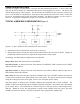
10 of 12
AC ELECTRICAL CHARACTERISTICS
(Over the operating range*)
PARAMETER SYMBOL MIN TYP MAX UNITS NOTES
SCL Clock Frequency f
SCL
0 100 kHz
Bus Free Time Between a STOP and
START Condition
t
BUF
4.7
ms
Hold Time (Repeated) START Condition t
HD:STA
4.0
ms
3
LOW Period of SCL Clock t
LOW
4.7
ms
HIGH Period of SCL Clock t
HIGH
4.0
ms
Set-up Time for a Repeated START
Condition
t
SU:STA
4.7
ms
Data Hold Time t
HD:DAT
0
ms
4,5
Data Set-up Time t
SU:DAT
250 ns
Rise Time of Both SDA and SCL Signals t
R
1000 ns
Fall Time of Both SDA and SCL Signals t
F
300 ns
Set-up Time for STOP Condition t
SU:STO
4.7
ms
Capacitive Load for each Bus Line C
B
400 pF 6
I/O Capacitance (T
A
= 25ºC)
C
I/O
10 pF
Crystal Specified Load Capacitance
(T
A
= 25ºC)
12.5 pF
*Unless otherwise specified.
NOTES:
1. I
CCS
specified with V
CC
= 5.0V and SDA, SCL = 5.0V.
2. V
CC
= 0V, V
BAT
= 3V.
3. After this period, the first clock pulse is generated.
4. A device must internally provide a hold time of at least 300ns for the SDA signal (referred to the
V
IHMIN
of the SCL signal) in order to bridge the undefined region of the falling edge of SCL.
5. The maximum t
HD:DAT
has only to be met if the device does not stretch the LOW period (t
LOW
) of the
SCL signal.
6. C
B
– Total capacitance of one bus line in pF.
7. I
CCA
– SCL clocking at max frequency = 100kHz.
8. V
PF
measured at V
BAT
= 3.0V.