
Data Sheet

LMV358
,
LMV321
,
LMV324
,
LMV324S
www.ti.com
SLOS263W –AUGUST 1999–REVISED OCTOBER 2014
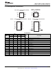
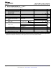
7.5 Electrical Characteristics: V
CC
+ = 2.7 V
V
CC+
= 2.7 V, T
A
= 25°C (unless otherwise noted)
PARAMETER TEST CONDITIONS MIN TYP
(1)
MAX UNIT
V
IO
Input offset voltage 1.7 7 mV
Average temperature coefficient of
α
VIO
5 μV/°C
input offset voltage
I
IB
Input bias current 11 250 nA
I
IO
Input offset current 5 50 nA
CMRR Common-mode rejection ratio V
CM
= 0 to 1.7 V 50 63 dB
k
SVR
Supply-voltage rejection ratio V
CC
= 2.7 V to 5 V, V
O
= 1 V 50 60 dB
0 –0.2
Common-mode input voltage
V
ICR
CMRR ≥ 50 dB V
range
1.9 1.7
High level V
CC
– 100 V
CC
– 10
V
O
Output swing R
L
= 10 kΩ to 1.35 V mV
Low level 60 180
LMV321I 80 170
LMV358I (both amplifiers) 140 340
I
CC
Supply current μA
LMV324I and LMV324SI
260 680
(all four amplifiers)
B
1
Unity-gain bandwidth C
L
= 200 pF 1 MHz
Φ
m
Phase margin 60 deg
G
m
Gain margin 10 dB
V
n
Equivalent input noise voltage f = 1 kHz 46 nV/√Hz
I
n
Equivalent input noise current f = 1 kHz 0.17 pA/√Hz
(1) Typical values represent the likely parametric nominal values determined at the time of characterization. Typical values depend on the
application and configuration and may vary over time. Typical values are not ensured on production material.
Copyright © 1999–2014, Texas Instruments Incorporated Submit Documentation Feedback 5
Product Folder Links: LMV358 LMV321 LMV324 LMV324S