
Data Sheet

LMV358
,
LMV321
,
LMV324
,
LMV324S
SLOS263W –AUGUST 1999–REVISED OCTOBER 2014
www.ti.com
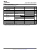
7 Specifications
7.1 Absolute Maximum Ratings
over operating free-air temperature range (unless otherwise noted)
(1)
MIN MAX UNIT
V
CC
Supply voltage
(2)
5.5 V
V
ID
Differential input voltage
(3)
±5.5 V
V
I
Input voltage range (either input) –0.2 5.7 V
At or below T
A
= 25°C,
Duration of output short circuit (one amplifier) to ground
(4)
Unlimited
V
CC
≤ 5.5 V
T
J
Operating virtual junction temperature 150 °C
(1) Stresses beyond those listed under Absolute Maximum Ratings may cause permanent damage to the device. These are stress ratings
only, and functional operation of the device at these or any other conditions beyond those indicated under Recommended Operating
Conditions is not implied. Exposure to absolute-maximum-rated conditions for extended periods may affect device reliability.
(2) All voltage values (except differential voltages and V
CC
specified for the measurement of I
OS
) are with respect to the network GND.
(3) Differential voltages are at IN+ with respect to IN–.
(4) Short circuits from outputs to V
CC
can cause excessive heating and eventual destruction.
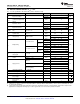
7.2 Handling Ratings
MIN MAX UNIT
T
stg
Storage temperature range –65 150 °C
Human body model (HBM), per ANSI/ESDA/JEDEC JS-001, all
0 2500
pins
(1)
V
(ESD)
Electrostatic discharge V
Charged device model (CDM), per JEDEC specification
0 1500
JESD22-C101, all pins
(2)
(1) JEDEC document JEP155 states that 500-V HBM allows safe manufacturing with a standard ESD control process.
(2) JEDEC document JEP157 states that 250-V CDM allows safe manufacturing with a standard ESD control process.
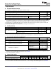
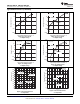
7.3 Recommended Operating Conditions
(1)
MIN MAX UNIT
V
CC
Supply voltage (single-supply operation) 2.7 5.5 V
V
CC
= 2.7 V 1.7
V
IH
Amplifier turn-on voltage level (LMV324S)
(2)
V
V
CC
= 5 V 3.5
V
CC
= 2.7 V 0.7
V
IL
Amplifier turn-off voltage level (LMV324S) V
V
CC
= 5 V 1.5
I temperature (LMV321,
LMV358, LMV324, –40 125
LMV321IDCK)
T
A
Operating free-air temperature °C
I temperature (LMV324S) -40 85
Q temperature –40 125
(1) All unused control inputs of the device must be held at V
CC
or GND to ensure proper device operation. See the TI application report,
Implications of Slow or Floating CMOS Inputs, literature number SCBA004.
(2) V
IH
should not be allowed to exceed V
CC
.
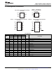
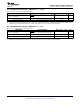
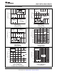
7.4 Thermal Information
LMV3xx
THERMAL METRIC
(1)
D DBV DCK DDU DGK PW UNIT
8 PIN 14 PIN 16 PIN 5 PIN 5 PIN 8 PIN 8 PIN 8 PIN 14 PIN 16 PIN
R
θJA
Junction-to-ambient thermal resistance 97 86 73 206 252 210 172 149 113 108 °C/W
(1) For more information about traditional and new thermal metrics, see the IC Package Thermal Metrics application report, SPRA953.
4 Submit Documentation Feedback Copyright © 1999–2014, Texas Instruments Incorporated
Product Folder Links: LMV358 LMV321 LMV324 LMV324S