
Data Sheet

0.0
0.5
1.0
1.5
2.0
2.5
3.0
0.0 0.5 1.0 1.5 2.0 2.5
VOUTt (V)
VIN (V)
C002
±2.5
±2.0
±1.5
±1.0
±0.5
0.0
0.5
1.0
1.5
2.0
2.5
0.0 0.5 1.0 1.5 2.0 2.5
VDIFF (V)
VIN (V)
C003
0.0
0.5
1.0
1.5
2.0
2.5
0.0 0.5 1.0 1.5 2.0 2.5
VOUT+ (V)
VIN (V)
C001
LMV358
,
LMV321
,
LMV324
,
LMV324S
SLOS263W –AUGUST 1999–REVISED OCTOBER 2014
www.ti.com
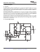
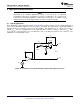
Typical Application (continued)
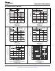
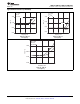
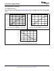
9.1.3 Application Curves
The measured transfer functions in Figure 47, Figure 48, and Figure 49 were generated by sweeping the input
voltage from 0 V to 2.5 V. However, this design should only be used between 0.5 V and 2 V for optimum
linearity.
Figure 47. Differential Output Voltage vs Input Voltage Figure 48. Positive Output Voltage Node vs Input Voltage
Figure 49. Positive Output Voltage Node vs Input Voltage
20 Submit Documentation Feedback Copyright © 1999–2014, Texas Instruments Incorporated
Product Folder Links: LMV358 LMV321 LMV324 LMV324S