
Data Sheet

OUT OUT
cm REF
V V
1
V V
2 2
+ -
+
æ ö
= =
ç ÷
è ø
2 4 2
D IF F O U T O U T IN R E F
1 3 4 1
R R R
V V V V 1 V 1
R R R R
+ -
æ ö
æ ö æ ö
= - = ´ + - ´ +
ç ÷
ç ÷ ç ÷
+
è ø è ø
è ø
4 2 2
out ref in
3 4 1 1
R R R
V V 1 V
R R R R
-
æ ö
æ ö
= ´ ´ + - ´
ç ÷
ç ÷
+
è ø
è ø
OUT REF
4
3
4
2
1 1
2
+
IN
LMV358
,
LMV321
,
LMV324
,
LMV324S
www.ti.com
SLOS263W –AUGUST 1999–REVISED OCTOBER 2014
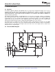
Typical Application (continued)
9.1.1 Design Requirements
The design requirements are as follows:
• Supply voltage: 2.7 V
• Reference voltage: 2.5 V
• Input: 0.5 to 2 V
• Output differential: ±1.5 V
9.1.2 Detailed Design Procedure
The circuit in Figure 46 takes a single-ended input signal, V
IN
, and generates two output signals, V
OUT+
and
V
OUT–
using two amplifiers and a reference voltage, V
REF
. V
OUT+
is the output of the first amplifier and is a
buffered version of the input signal, V
IN
(see Equation 1). V
OUT–
is the output of the second amplifier which uses
V
REF
to add an offset voltage to V
IN
and feedback to add inverting gain. The transfer function for V
OUT–
is
Equation 2.
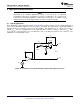
V
OUT+
= V
IN
(1)
(2)
The differential output signal, V
DIFF
, is the difference between the two single-ended output signals, V
OUT+
and
V
OUT–
. Equation 3 shows the transfer function for V
DIFF
. By applying the conditions that R
1
= R
2
and R
3
= R
4
, the
transfer function is simplified into Equation 6. Using this configuration, the maximum input signal is equal to the
reference voltage and the maximum output of each amplifier is equal to the V
REF
. The differential output range is
2×V
REF
. Furthermore, the common mode voltage will be one half of V
REF
(see Equation 7).
(3)
V
OUT+
= V
IN
(4)
V
OUT–
= V
REF
– V
IN
(5)
V
DIFF
= 2×V
IN
– V
REF
(6)
(7)
9.1.2.1 Amplifier Selection
Linearity over the input range is key for good dc accuracy. The common mode input range and the output swing
limitations determine the linearity. In general, an amplifier with rail-to-rail input and output swing is required.
Bandwidth is a key concern for this design. Because LMV358 has a bandwidth of 1 MHz, this circuit will only be
able to process signals with frequencies of less than 1 MHz.
9.1.2.2 Passive Component Selection
Because the transfer function of V
OUT–
is heavily reliant on resistors (R
1
, R
2
, R
3
, and R
4
), use resistors with low
tolerances to maximize performance and minimize error. This design used resistors with resistance values of
36 kΩ with tolerances measured to be within 2%. If the noise of the system is a key parameter, the user can
select smaller resistance values (6 kΩ or lower) to keep the overall system noise low. This ensures that the noise
from the resistors is lower than the amplifier noise.
Copyright © 1999–2014, Texas Instruments Incorporated Submit Documentation Feedback 19
Product Folder Links: LMV358 LMV321 LMV324 LMV324S