
Data Sheet
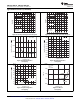

R3
R1
R2
R4
2.7 V
VREF
2.5 V
+
+
VIN
+
VDIFF
±
VOUT-
VOUT+
LMV358
,
LMV321
,
LMV324
,
LMV324S
SLOS263W –AUGUST 1999–REVISED OCTOBER 2014
www.ti.com
9 Application and Implementation
NOTE
Information in the following applications sections is not part of the TI component
specification, and TI does not warrant its accuracy or completeness. TI’s customers are
responsible for determining suitability of components for their purposes. Customers should
validate and test their design implementation to confirm system functionality.
9.1 Typical Application
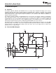
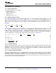
Some applications require differential signals. Figure 46 shows a simple circuit to convert a single-ended input of
0.5 to 2 V into differential output of ±1.5 V on a single 2.7-V supply. The output range is intentionally limited to
maximize linearity. The circuit is composed of two amplifiers. One amplifier acts as a buffer and creates a
voltage, V
OUT+
. The second amplifier inverts the input and adds a reference voltage to generate V
OUT–
. Both
V
OUT+
and V
OUT–
range from 0.5 to 2 V. The difference, V
DIFF
, is the difference between V
OUT+
and V
OUT–
. The
LMV358 was used to build this circuit.
Figure 46. Schematic for Single-Ended Input to Differential Output Conversion
18 Submit Documentation Feedback Copyright © 1999–2014, Texas Instruments Incorporated
Product Folder Links: LMV358 LMV321 LMV324 LMV324S