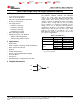
Product Folder Sample & Buy Tools & Software Technical Documents Support & Community LMV358, LMV321, LMV324, LMV324S SLOS263W – AUGUST 1999 – REVISED OCTOBER 2014 LMV3xx Low-Voltage Rail-to-Rail Output Operational Amplifiers 1 Features 3 Description • • • • • The LMV321, LMV358, LMV324, and LMV324S devices are single, dual, and quad low-voltage (2.7 V to 5.5 V) operational amplifiers with rail-to-rail output swing.
LMV358, LMV321, LMV324, LMV324S SLOS263W – AUGUST 1999 – REVISED OCTOBER 2014 www.ti.com Table of Contents 1 2 3 4 5 6 7 Features .................................................................. Applications ........................................................... Description ............................................................. Simplified Schematic............................................. Revision History.....................................................
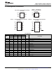
LMV358, LMV321, LMV324, LMV324S www.ti.com SLOS263W – AUGUST 1999 – REVISED OCTOBER 2014 6 Pin Configuration and Functions LMV358 . . . D (SOIC), DDU (VSSOP), DGK (VSSOP), OR PW (TSSOP) PACKAGE (TOP VIEW) 1OUT 1IN– 1IN+ GND 1 8 2 7 3 6 4 5 VCC+ 2OUT 2IN– 2IN+ LMV324 . . . D (SOIC) OR PW (TSSOP) PACKAGE (TOP VIEW) 1OUT 1IN– 1IN+ VCC+ 2IN+ 2IN– 2OUT 1 14 2 13 3 12 4 11 5 10 6 9 7 8 LMV321 . . .
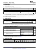
LMV358, LMV321, LMV324, LMV324S SLOS263W – AUGUST 1999 – REVISED OCTOBER 2014 www.ti.com 7 Specifications 7.1 Absolute Maximum Ratings over operating free-air temperature range (unless otherwise noted) (1) MIN (3) VID Differential input voltage VI Input voltage range (either input) –0.2 Duration of output short circuit (one amplifier) to ground (4) TJ (1) (2) (3) (4) MAX Supply voltage (2) VCC At or below TA = 25°C, VCC ≤ 5.5 V UNIT 5.5 V ±5.5 V 5.
LMV358, LMV321, LMV324, LMV324S www.ti.com SLOS263W – AUGUST 1999 – REVISED OCTOBER 2014 7.5 Electrical Characteristics: VCC+ = 2.7 V VCC+ = 2.7 V, TA = 25°C (unless otherwise noted) PARAMETER TEST CONDITIONS MIN TYP (1) MAX 1.7 7 UNIT VIO Input offset voltage αVIO Average temperature coefficient of input offset voltage IIB Input bias current IIO Input offset current CMRR Common-mode rejection ratio VCM = 0 to 1.7 V 50 63 dB kSVR Supply-voltage rejection ratio VCC = 2.
LMV358, LMV321, LMV324, LMV324S SLOS263W – AUGUST 1999 – REVISED OCTOBER 2014 www.ti.com 7.6 Electrical Characteristics: VCC+ = 5 V VCC+ = 5 V, at specified free-air temperature (unless otherwise noted) PARAMETER TEST CONDITIONS TA (1) MIN 25°C TYP (2) MAX 1.
LMV358, LMV321, LMV324, LMV324S www.ti.com SLOS263W – AUGUST 1999 – REVISED OCTOBER 2014 7.7 Shutdown Characteristics, LMV324S: VCC+ = 2.7 V VCC+ = 2.7 V, TA = 25°C (unless otherwise noted) PARAMETER TEST CONDITIONS MIN TYP (1) MAX UNIT ICC(SHDN) Supply current in shutdown mode (per channel) SHDN ≤ 0.
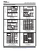
LMV358, LMV321, LMV324, LMV324S SLOS263W – AUGUST 1999 – REVISED OCTOBER 2014 www.ti.com 7.9 Typical Characteristics Vs = 2.7 V RL = 100 kΩ, 2 kΩ, 600 Ω 70 Phase 60 Gain − dB 40 100 kΩ Gain 70 90 60 75 60 2 kΩ 30 105 45 20 30 600 Ω 10 100 kΩ −10 1k 10 k 600 Ω Phase 75 2 kΩ 40 100 k Frequency − Hz 30 45 Gain 20 10 15 1M 0 0 −15 10 M −10 1k 70 10 k 70 100 Phase 0 pF 80 −20 −20 Vs = 5.
LMV358, LMV321, LMV324, LMV324S www.ti.com SLOS263W – AUGUST 1999 – REVISED OCTOBER 2014 Typical Characteristics (continued) 10000 10000 VCC = ±2.5 V RL = 2 kΩ AV = 10 VO = 100 mVPP 2.5 V _ 1000 VO + RL CL Capacitive Load − nF Capacitive Load − pF VI 2.5 V LMV324S (25% Overshoot) 100 10 −2.0 −1.5 1000 LMV3xx (25% Overshoot) 100 134 kΩ −1 −0.5 0 Output Voltage − V 0.5 1 1.21 MΩ +2.5 V VCC = ±2.5 V AV = +1 RL = 1 MΩ VO = 100 mVPP LMV3xx (25% Overshoot) _ 10 −2.0 1.5 −1.5 −1 −0.
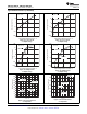
LMV358, LMV321, LMV324, LMV324S SLOS263W – AUGUST 1999 – REVISED OCTOBER 2014 www.ti.com Typical Characteristics (continued) 100 100 VCC = 2.7 V VCC = 5 V 10 Sourcing Current − mA Sourcing Current − mA 10 LMV3xx 1 LMV324S 0.1 LMV3xx 1 LMV324S 0.1 0.01 0.01 0.001 0.001 0.01 0.1 1 0.001 0.001 10 Figure 13. Source Current vs Output Voltage 10 LMV324S Sinking Current − mA LMV324S 1 LMV3xx 0.1 1 LMV324 0.1 0.01 0.01 0.01 0.1 1 10 0.001 0.
LMV358, LMV321, LMV324, LMV324S www.ti.com SLOS263W – AUGUST 1999 – REVISED OCTOBER 2014 Typical Characteristics (continued) 80 90 LMV324S VCC = −5 V RL = 10 kΩ 70 VCC = 5 V RL = 10 kΩ 70 60 LMV3xx LMV3xx 60 50 +k SVR − dB −k SVR − dB LMV324S 80 40 30 50 40 30 20 20 10 10 0 0 100 1k 10k 100k 1M 1k Figure 20. +kSVR vs Frequency 80 VCC = −2.7 V RL = 10 kΩ LMV324S 70 60 1M VCC = 2.
LMV358, LMV321, LMV324, LMV324S SLOS263W – AUGUST 1999 – REVISED OCTOBER 2014 www.ti.com Typical Characteristics (continued) 150 110 LMV3xx VCC = 5 V Impedance − Ω 90 80 70 LMV324S VCC = 2.7 V 60 50 LMV324S VCC = 5 V 40 VCC = 5 V RL = 5 kΩ AV = 1 VO = 3 VPP 140 Crosstalk Rejection − dB 100 LMV3xx VCC = 2.7 V 130 120 110 100 30 20 1 1M 2M 3M 90 100 4M Frequency − Hz 1k 10k Frequency − Hz Figure 25. Open-Loop Output Impedence vs Frequency Figure 26.
LMV358, LMV321, LMV324, LMV324S www.ti.com SLOS263W – AUGUST 1999 – REVISED OCTOBER 2014 Typical Characteristics (continued) Input Input 50 mV/Div 50 mV/Div LMV3xx LMV3xx LMV324S LMV324S VCC = ±2.5 V RL = 2 kΩ TA = 85°C VCC = ±2.5 V RL = 2 kΩ TA = −40°C 1 µs/Div Figure 32. Noninverting Small-Signal Pulse Response 1 µs/Div Figure 31. Noninverting Small-Signal Pulse Response Input Input LMV3xx 1 V/Div 1 V/Div LMV3xx LMV324S LMV324S VCC = ±2.5 V RL = 2 kΩ TA = 25°C VCC = ±2.
LMV358, LMV321, LMV324, LMV324S SLOS263W – AUGUST 1999 – REVISED OCTOBER 2014 www.ti.com Input Input LMV3xx LMV3xx 50 mV/Div 50 mV/Div Typical Characteristics (continued) LMV324S LMV324S VCC = ±2.5 V RL = 2 kΩ TA = −40°C VCC = ±2.5 V RL = 2 kΩ TA = 85°C 1 µs/Div 1 µs/Div Figure 37. Inverting Small-Signal Pulse Response Figure 38. Inverting Small-Signal Pulse Response 0.50 0.80 0.60 0.40 0.20 VCC = 5 V 0.45 Input Current Noise − pA/ Hz Input Current Noise − pA/ Hz VCC = 2.7 V 0.40 0.
LMV358, LMV321, LMV324, LMV324S www.ti.com SLOS263W – AUGUST 1999 – REVISED OCTOBER 2014 Typical Characteristics (continued) 10.000 10.000 VCC = 2.7 V RL = 10 kΩ AV = 10 VO = 1 VPP 1.000 1.000 VCC = 5 V RL = 10 kΩ AV = 1 VO = 1 VPP THD − % THD − % LMV324S 0.100 LMV3xx 0.100 LMV324S 0.010 0.010 LMV3xx 0.001 0.001 10 100 1000 10000 10 100000 1000 100 Frequency − Hz 10000 100000 Frequency − Hz Figure 43. THD + N vs Frequency Figure 44. THD + N vs Frequency 10.
LMV358, LMV321, LMV324, LMV324S SLOS263W – AUGUST 1999 – REVISED OCTOBER 2014 www.ti.com 8 Detailed Description 8.1 Overview The LMV321, LMV358, LMV324, and LMV324S devices are single, dual, and quad low-voltage (2.7 V to 5.5 V) operational amplifiers with rail-to-rail output swing. The LMV324S device, which is a variation of the standard LMV324 device, includes a power-saving shutdown feature that reduces supply current when the amplifiers are not needed.
LMV358, LMV321, LMV324, LMV324S www.ti.com SLOS263W – AUGUST 1999 – REVISED OCTOBER 2014 8.3 Feature Description 8.3.1 Operating Voltage The LMV321, LMV358, LMV324, LMV324S devices are fully specified and ensured for operation from 2.7 V to 5 V. In addition, many specifications apply from –40°C to 125°C. Parameters that vary significantly with operating voltages or temperature are shown in the Typical Characteristics graphs. 8.3.
LMV358, LMV321, LMV324, LMV324S SLOS263W – AUGUST 1999 – REVISED OCTOBER 2014 www.ti.com 9 Application and Implementation NOTE Information in the following applications sections is not part of the TI component specification, and TI does not warrant its accuracy or completeness. TI’s customers are responsible for determining suitability of components for their purposes. Customers should validate and test their design implementation to confirm system functionality. 9.
LMV358, LMV321, LMV324, LMV324S www.ti.com SLOS263W – AUGUST 1999 – REVISED OCTOBER 2014 Typical Application (continued) 9.1.1 Design Requirements The design requirements are as follows: • Supply voltage: 2.7 V • Reference voltage: 2.5 V • Input: 0.5 to 2 V • Output differential: ±1.5 V 9.1.2 Detailed Design Procedure The circuit in Figure 46 takes a single-ended input signal, VIN, and generates two output signals, VOUT+ and VOUT– using two amplifiers and a reference voltage, VREF.
LMV358, LMV321, LMV324, LMV324S SLOS263W – AUGUST 1999 – REVISED OCTOBER 2014 www.ti.com Typical Application (continued) 9.1.3 Application Curves The measured transfer functions in Figure 47, Figure 48, and Figure 49 were generated by sweeping the input voltage from 0 V to 2.5 V. However, this design should only be used between 0.5 V and 2 V for optimum linearity. 2.5 2.5 2.0 1.5 2.0 VOUT+ (V) VDIFF (V) 1.0 0.5 0.0 ±0.5 1.5 1.0 ±1.0 0.5 ±1.5 ±2.0 0.0 ±2.5 0.0 0.5 1.0 1.5 2.0 0.0 2.
LMV358, LMV321, LMV324, LMV324S www.ti.com SLOS263W – AUGUST 1999 – REVISED OCTOBER 2014 10 Power Supply Recommendations The LMV321, LMV358, LMV324, LMV324S devices are specified for operation from 2.7 to 5 V; many specifications apply from –40°C to 125°C. The Typical Characteristics section presents parameters that can exhibit significant variance with regard to operating voltage or temperature. CAUTION Supply voltages larger than 5.
LMV358, LMV321, LMV324, LMV324S SLOS263W – AUGUST 1999 – REVISED OCTOBER 2014 www.ti.com 11 Layout 11.1 Layout Guidelines For best operational performance of the device, use good PCB layout practices, including: • Noise can propagate into analog circuitry through the power pins of the circuit as a whole, as well as the operational amplifier. Bypass capacitors are used to reduce the coupled noise by providing low impedance power sources local to the analog circuitry. – Connect low-ESR, 0.
LMV358, LMV321, LMV324, LMV324S www.ti.com SLOS263W – AUGUST 1999 – REVISED OCTOBER 2014 12 Device and Documentation Support 12.1 Related Links The table below lists quick access links. Categories include technical documents, support and community resources, tools and software, and quick access to sample or buy. Table 1.
PACKAGE OPTION ADDENDUM www.ti.
PACKAGE OPTION ADDENDUM www.ti.
PACKAGE OPTION ADDENDUM www.ti.
PACKAGE OPTION ADDENDUM www.ti.com 16-Nov-2015 (2) Eco Plan - The planned eco-friendly classification: Pb-Free (RoHS), Pb-Free (RoHS Exempt), or Green (RoHS & no Sb/Br) - please check http://www.ti.com/productcontent for the latest availability information and additional product content details. TBD: The Pb-Free/Green conversion plan has not been defined.
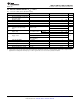
PACKAGE MATERIALS INFORMATION www.ti.com 20-Aug-2015 TAPE AND REEL INFORMATION *All dimensions are nominal Device Package Package Pins Type Drawing SPQ Reel Reel A0 Diameter Width (mm) (mm) W1 (mm) B0 (mm) K0 (mm) P1 (mm) LMV321IDBVR SOT-23 DBV 5 3000 178.0 9.0 LMV321IDBVT SOT-23 DBV 5 250 180.0 LMV321IDBVT SOT-23 DBV 5 250 178.
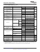
PACKAGE MATERIALS INFORMATION www.ti.com 20-Aug-2015 Device Package Package Pins Type Drawing SPQ Reel Reel A0 Diameter Width (mm) (mm) W1 (mm) B0 (mm) K0 (mm) P1 (mm) W Pin1 (mm) Quadrant LMV358IDR SOIC D 8 2500 330.0 12.4 6.4 5.2 2.1 8.0 12.0 Q1 LMV358IDR SOIC D 8 2500 330.0 12.4 6.4 5.2 2.1 8.0 12.0 Q1 LMV358IDR SOIC D 8 2500 330.0 12.8 6.4 5.2 2.1 8.0 12.0 Q1 LMV358IDRG4 SOIC D 8 2500 330.0 12.4 6.4 5.2 2.1 8.0 12.
PACKAGE MATERIALS INFORMATION www.ti.com 20-Aug-2015 Device Package Type Package Drawing Pins SPQ Length (mm) Width (mm) Height (mm) LMV324IDR SOIC D 14 2500 364.0 364.0 27.0 LMV324IDR SOIC D 14 2500 367.0 367.0 38.0 LMV324IDR SOIC D 14 2500 333.2 345.9 28.6 LMV324IDRG4 SOIC D 14 2500 333.2 345.9 28.6 LMV324IPWR TSSOP PW 14 2000 364.0 364.0 27.0 LMV324IPWR TSSOP PW 14 2000 367.0 367.0 35.0 LMV324IPWRG4 TSSOP PW 14 2000 367.0 367.0 35.
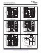
PACKAGE OUTLINE PW0008A TSSOP - 1.2 mm max height SCALE 2.800 SMALL OUTLINE PACKAGE C 6.6 TYP 6.2 SEATING PLANE PIN 1 ID AREA A 0.1 C 6X 0.65 8 1 3.1 2.9 NOTE 3 2X 1.95 4 5 B 4.5 4.3 NOTE 4 SEE DETAIL A 8X 0.30 0.19 0.1 C A 1.2 MAX B (0.15) TYP 0.25 GAGE PLANE 0 -8 0.15 0.05 0.75 0.50 DETAIL A TYPICAL 4221848/A 02/2015 NOTES: 1. All linear dimensions are in millimeters. Any dimensions in parenthesis are for reference only. Dimensioning and tolerancing per ASME Y14.5M. 2.
EXAMPLE BOARD LAYOUT PW0008A TSSOP - 1.2 mm max height SMALL OUTLINE PACKAGE 8X (1.5) 8X (0.45) SYMM 1 8 (R0.05) TYP SYMM 6X (0.65) 5 4 (5.8) LAND PATTERN EXAMPLE SCALE:10X SOLDER MASK OPENING METAL SOLDER MASK OPENING METAL UNDER SOLDER MASK 0.05 MAX ALL AROUND 0.05 MIN ALL AROUND SOLDER MASK DEFINED NON SOLDER MASK DEFINED SOLDER MASK DETAILS NOT TO SCALE 4221848/A 02/2015 NOTES: (continued) 6. Publication IPC-7351 may have alternate designs. 7.
EXAMPLE STENCIL DESIGN PW0008A TSSOP - 1.2 mm max height SMALL OUTLINE PACKAGE 8X (1.5) 8X (0.45) SYMM (R0.05) TYP 1 8 SYMM 6X (0.65) 5 4 (5.8) SOLDER PASTE EXAMPLE BASED ON 0.125 mm THICK STENCIL SCALE:10X 4221848/A 02/2015 NOTES: (continued) 8. Laser cutting apertures with trapezoidal walls and rounded corners may offer better paste release. IPC-7525 may have alternate design recommendations. 9. Board assembly site may have different recommendations for stencil design. www.ti.
IMPORTANT NOTICE Texas Instruments Incorporated and its subsidiaries (TI) reserve the right to make corrections, enhancements, improvements and other changes to its semiconductor products and services per JESD46, latest issue, and to discontinue any product or service per JESD48, latest issue. Buyers should obtain the latest relevant information before placing orders and should verify that such information is current and complete.