
Data Sheet

Rev 0 5
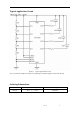
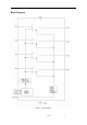
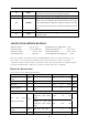
12 HYS2
Input of Comparator hysteresis (Hysteresis) to set. Logic
inputs, HYS1 and HYS2 set the comparator hysteresis .
13 GND Negative Terminal of Power Supply(Ground)
14 BLINK
Input of flash output control. Logic input, when the comparator
output is low, the comparator flip CHRG threshold control input
is low, and BLINK pin is high, the comparator output is about 500
ms conversion time at intervals , the duration of high and low the
same.
15 NC No Connection.
16 VDD
Positive Terminal of Power Supply. This pin is the power supply
to internal circuit.
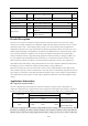
ABSOLUTE MAXIMUM RATINGS
VDD Pin voltage..............… -0.3V to +6.5V
Input Pin voltage………….-0.3V to VDD+0.3V
Output Pin voltage………………-0.3V to 6.5V
Thermal Resistance………………300°C/W
Maximum Junction Temperature…150°C
Operating Temperature.…..……...-40 to +85°C
Storage Temperature.......…….......-65 to +150°C
Lead Temperature (soldering, 10s) .......+260°
Stresses beyond those listed under “Absolute Maximum Ratings” may cause permanent damage to the
device. These are stress ratings only, and functional operation of the device at these or any other
conditions beyond those indicated in the operational sections of the specifications is not implied. Exposure
to absolute maximum rating conditions for extended periods may affect device reliability.
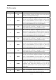
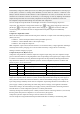
Electrical Characteristics
(V
CC
=3.7V, T
A
= 25℃, unless otherwise noted.)
Parameters Symbol Test Conditions Min Typ Max Unit
Operating Voltage
Range
V
CC
2.7 6 V
Operating Current I
VCC
V
CC
=3.7V
7.3 uA
Start time 7.5 15 22.5 ms
Flicker frequency
CHRG is low, BLINK is
high
2 Hz
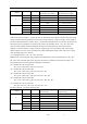
Comparator
CHRG is high, the
comparator input voltage
drops
1.189 1.22 1.25
The flip down
comparator threshold
Vtrip
CHRG is low, the
comparator input voltage
drops
1.22 1.256 1.29
V
Negative input bias
current
I
bias
IN1,IN2,IN3,IN4 0 50 nA
Comparator delay t
PD