
User Manual
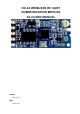

HC‐12WIRELESSRFUARTCOMMUNICATIONMODULEV2.4USERMANUAL
WEB:www.hc01.com
PAGE 2
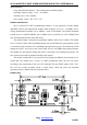
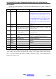
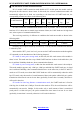
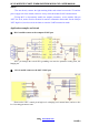
Pin definition
The HC-12 module consists of 9 pins and a RF antenna block ANT1, which is defined as
the following table:
pin definition I/O explain
1 VCC
Power pin, the requirements of 3.2V to 5.5V
DC power supply, the supply current is not less
than 200mA.(Note: If the module is to work
for a long time in the transmit state, it is
recommended that the power supply voltage
of more than 4.5V when connected to a
1N4007 diode, to avoid the module built-in
LDO fever.)
2 GND Ground
3 RXD input, with pull up resistor
to internal power supply
UART input, 3.3V TTL level
, internal 1K
resistor in series
4 TXD Output, with pull up resistor
to external VCC
UART output, 3.3V TTL level
,internal 1K
resistor in series
5 SET input, internal 10K pull up
resistor
Parameter setting pin, the low level is
effective, internal 1K resistor in series
6 ANT RF input/output 433MHz antenna pin
7 GND Ground
8 GND Ground
9 NC NC
ANT1 ANT RF input/output IPEX20279-001E-03 antenna seat
ANT2 ANT RF input/output 433MHz spring antenna welding hole
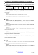
Pin1- 6 have two pads each, by the outside of the half hole pad for the patch welding. Pin 6
on the inside of the pad ANT2 for module chip welding, you can hand welding spring antenna.
Pin 1 - 5 by hole inside the pads used for welding 2.54mm row spacing, can be plugged directly
into the user PCB row seat.