
Data Sheet


Page 87
RFM95/96/97/98
Tel: +86-755-82973805 Fax: +86-755-82973550 E-mail: sales@hoperf.com http:/ / www.hoperf.com
WIRELESS & SENSING PRELIMINARY DATASHEET
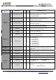
6.2. FSK/OOK Mode Register Map
This section details the RFM95/96/97/98 register mapping and the precise contents of each register in FSK/OOK
mode. Convention: r: read, w: write, t:trigger, c: clear
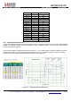
Table 86 Register Map
Name
(Address)
Bits
Variable Name
Mode
Default
value
FSK/OOK Description
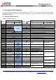
RegFifo
(0x00)
7-0
Fifo
rw
0x00
FIFO data input/output
Registers for Common settings
7
LongRangeMode
r
0x00
0 FSK/OOK Mode
1
LoRa
TM
Mode
This bit can be modified only in Sleep mode. A write operation on
other device modes is ignored.
6-5
ModulationType
rw
0x00
Modulation scheme:
00 FSK
01 OOK
10 11 reserved
4 reserved r 0x0 reserved
3
LowFrequencyModeOn
rw
0x01
Access Low Frequency Mode registers (from address 0x61 on)
0 High Frequency Mode (access to HF test registers)
1 Low Frequency Mode (access to LF test registers)
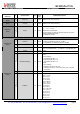
RegOpMode
(0x01)
2-0
Mode
rw
0x01
Transceiver modes
000 Sleep mode
001 Stdby mode
010 FS mode TX (FSTx)
011 Transmitter mode (Tx)
100 FS mode RX (FSRx)
101 Receiver mode (Rx)
110 reserved
111 reserved
RegBitrateMsb
(0x02)
7-0
BitRate(15:8)
rw
0x1a
MSB of Bit Rate (chip rate if Manchester encoding is enabled)
RegBitrateLsb
(0x03)
7-0
BitRate(7:0)
rw
0x0b
LSB of bit rate (chip rate if Manchester encoding is enabled)
BitRate =
---------------------------
F
----
X
----
O
-----
S
---
C
------------------------------
Bi tR ate(15,0) +
-
B
----
i
--
t
--
r
--
a
----
t
--
e
---
F
----
r
--
a
----
c
-
16
Default value: 4.8 kb/s
7-6 reserved rw 0x00 reserved
RegFdevMsb
(0x04)
5-0 Fdev(13:8) rw 0x00 MSB of the frequency deviation
RegFdevLsb
(0x05)
7-0
Fdev(7:0)
rw
0x52
LSB of the frequency deviation
Fdev = Fste p
×
Fdev(15,0)
Default value: 5 kHz