
Data Sheet

Page 19
RFM95/96/97/98
Te l : + 8 6 - 7 5 5 - 8 2 9 7 3 8 0 5 Fa x : + 8 6 - 7 5 5 - 8 2 9 7 3 5 5 0 E- m a i l : sa l e s @ h o p e r f . c o m h t t p : / / w w w . h o p e r f . c o m
WIRELESS & SENSING PRELIMINARY DATASHEET
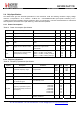
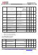
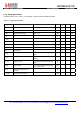
2.4.6. Digital Specification
Conditions: Temp = 25° C, VDD = 3.3 V, FXOSC = 32 MHz, unless otherwise specified.
Table 57 Digital Specification
Symbol
Description
Conditions
Min
Typ
Max
Unit
V
IH
Digital input level high
0.8 - - VDD
V
IL
Digital input level low
- - 0.2 VDD
V
OH
Digital output level high Imax = 1 mA 0.9 - - VDD
V
OL
Digital output level low Imax = -1 mA - - 0.1 VDD
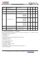
F
SCK
SCK frequency
- - 10 MHz
t
ch
SCK high time
50 - - ns
t
cl
SCK low time
50 - - ns
t
rise
SCK rise time
- 5 - ns
t
fall
SCK fall time
- 5 - ns
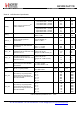
t
setup
MOSI setup time From MOSI change to SCK rising
edge.
30 - - ns
t
hold
MOSI hold time From SCK rising edge to MOSI
change.
20 - - ns
t
nsetup
NSS setup time From NSS falling edge to SCK rising
edge.
30 - - ns
t
nhold
NSS hold time From SCK falling edge to NSS rising
edge, normal mode.
100 - - ns
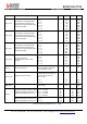
t
nhigh
NSS high time between SPI
accesses
20 - - ns
T_DATA DATA hold and setup time
250 - - ns