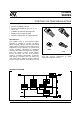
L78M00 SERIES POSITIVE VOLTAGE REGULATORS ■ OUTPUT CURRENT TO 0.5A ■ OUTPUT VOLTAGES OF 5; 6; 8; 9; 12; 15; 18; 20; 24V ■ THERMAL OVERLOAD PROTECTION ■ SHORT CIRCUIT PROTECTION ■ OUTPUT TRANSITION SOA PROTECTION TO-220 TO-220FP DESCRIPTION The L78M00 series of three-terminal positive regulators is available in TO-220, TO-220FP, DPAK and IPAK packages and with several fixed output voltages, making it useful in a wide range of applications.
L78M00 SERIES ABSOLUTE MAXIMUM RATINGS Symbol VI Parameter DC Input Voltage Value Unit 35 40 V V (for VO= 5 to 18V) (for VO= 20, 24V) IO Output Current Internally Limited mA Internally Limited mW -65 to +150 °C 0 to +150 °C PD Power Dissipation Tstg Storage Temperature Range Top Operating Junction Temperature Range Absolute Maximum Ratings are those values beyond which damage to the device may occur. Functional operation under these condition is not implied.
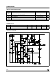
L78M00 SERIES CONNECTION DIAGRAM (top view) TO-220 TO-220FP DPAK IPAK ORDERING CODES TYPE TO-220 TO-220FP DPAK (*) IPAK OUTPUT VOLTAGE L78M05 L78M06 L78M08 L78M09 L78M10 L78M12 L78M15 L78M18 L78M20 L78M24 L78M05CV L78M06CV L78M08CV L78M09CV L78M10CV L78M12CV L78M15CV L78M18CV L78M20CV L78M24CV L78M05CP L78M06CP L78M08CP L78M09CP L78M10CP L78M12CP L78M15CP L78M18CP L78M20CP L78M24CP L78M05CDT L78M06CDT L78M08CDT L78M09CDT L78M10CDT L78M12CDT L78M15CDT L78M18CDT L78M20CDT L78M24CDT L78M05CDT-1
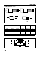
L78M00 SERIES TEST CIRCUITS Figure 1 : DC Parameter Figure 2 : Load Regulation Figure 3 : Ripple Rejection 4/21
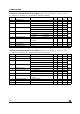
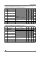
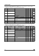
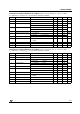
L78M00 SERIES ELECTRICAL CHARACTERISTICS OF L78M05C (refer to the test circuits, TJ = 25°C, VI = 10V, IO = 350 mA, CI = 0.33 µF, CO = 0.1 µF unless otherwise specified). Symbol Parameter VO Output Voltage VO Output Voltage ∆VO Line Regulation ∆VO Id ∆Id Load Regulation Test Conditions IO = 5 to 350 mA VI = 7 to 20 V Min. Typ. 4.8 5 5.2 V 5 5.
L78M00 SERIES ELECTRICAL CHARACTERISTICS OF L78M08C (refer to the test circuits, TJ = 25°C, VI = 14V, IO = 350 mA, CI = 0.33 µF, CO = 0.1 µF unless otherwise specified). Symbol Parameter VO Output Voltage Test Conditions Min. Typ. Max. Unit 7.7 8 8.3 V 7.6 8 VO Output Voltage IO = 5 to 350 mA VI = 10.5 to 23 V ∆VO Line Regulation VI = 10.
L78M00 SERIES ELECTRICAL CHARACTERISTICS OF L78M10C (refer to the test circuits, TJ = 25°C, VI = 16V, IO = 350 mA, CI = 0.33 µF, CO = 0.1 µF unless otherwise specified). Symbol Parameter VO Output Voltage VO Output Voltage ∆VO Line Regulation ∆VO Id ∆Id Load Regulation Test Conditions IO = 5 to 350 mA VI = 12.5 to 25 V Min. Typ. Max. Unit 9.6 10 10.4 V 9.5 10 10.5 V mV VI = 12.
L78M00 SERIES ELECTRICAL CHARACTERISTICS OF L78M15C (refer to the test circuits, TJ = 25°C, VI = 23V, IO = 350 mA, CI = 0.33 µF, CO = 0.1 µF unless otherwise specified). Symbol Parameter VO Output Voltage VO Output Voltage ∆VO Line Regulation ∆VO Id ∆Id Load Regulation IO = 5 to 350 mA VI = 17.5 to 30 V Min. Typ. Max. Unit 14.4 14.25 15 15.6 V 15 15.75 V mV VI = 17.
L78M00 SERIES ELECTRICAL CHARACTERISTICS OF L78M20C (refer to the test circuits, TJ = 25°C, VI = 29V, IO = 350 mA, CI = 0.33 µF, CO = 0.1 µF unless otherwise specified). Symbol Parameter VO Output Voltage VO Output Voltage ∆VO Line Regulation ∆VO Id ∆Id Load Regulation Test Conditions IO = 5 to 350 mA VI = 23 to 35 V Min. Typ. Max. Unit 19.2 20 20.
L78M00 SERIES Figure 4 : Dropout Voltage vs Junction Temperature Figure 7 : Output Voltage vs Junction Temperature Figure 5 : Dropout Characteristics Figure 8 : Supply Voltage Rejection vs Frequency Figure 6 : Peak Output Current vs Input-Output Differential Voltage Figure 9 : Quiescent Current vs Junction Temperature 10/21
L78M00 SERIES Figure 10 : Load Transient Response Figure 12 : Quiescent Current vs Input Voltage Figure 11 : Line Transient Response 11/21
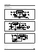
L78M00 SERIES Figure 13 : Fixed Output Regulator NOTE: 1. To specify an output voltage, substitute voltage value for "XX". 2. Although no output capacitor is need for stability, it does improve transient response. 3. Required if regulator is locate an appreciable distance from power supply filter.
L78M00 SERIES Figure 16 : Adjustable Output Regulator (7 to 30V) Figure 17 : 0.
L78M00 SERIES Figure 20 : Tracking Voltage Regulator Figure 21 : High Input Voltage Circuit VIN = VI - (VZ + VBE) Figure 22 : Reducing Power Dissipation with Dropping Resistor VI(min) - VXX - VDROP(max) R = IO(max) + Id(max) 14/21
L78M00 SERIES Figure 23 : Power AM Modulator (unity voltage gain, IO ≤ 0.5) NOTE: The circuit performs well up to 100 KHz. Figure 24 : Adjustable Output Voltage with Temperature Compensation R2 VO = VXX (1+ ) + VBE R1 NOTE: Q2 is connected as a diode in order to compensate the variation of the Q1 VBE with the temperature. C allows a slow risetime of the VO.
L78M00 SERIES TO-220 MECHANICAL DATA DIM. mm. MIN. TYP inch MAX. MIN. TYP. MAX. A 4.40 4.60 0.173 0.181 C 1.23 1.32 0.048 0.051 D 2.40 2.72 0.094 0.107 D1 1.27 0.050 E 0.49 0.70 0.019 0.027 F 0.61 0.88 0.024 0.034 F1 1.14 1.70 0.044 0.067 F2 1.14 1.70 0.044 0.067 G 4.95 5.15 0.194 0.203 G1 2.4 2.7 0.094 0.106 H2 10.0 10.40 0.393 0.409 L2 16.4 0.645 L4 13.0 14.0 0.511 0.551 L5 2.65 2.95 0.104 0.116 L6 15.25 15.75 0.600 0.
L78M00 SERIES TO-220FP MECHANICAL DATA mm. DIM. MIN. inch TYP MAX. MIN. TYP. MAX. A 4.40 4.60 0.173 0.181 B 2.5 2.7 0.098 0.106 D 2.5 2.75 0.098 0.108 E 0.45 0.70 0.017 0.027 F 0.75 1 0.030 0.039 F1 1.15 1.50 0.045 0.059 F2 1.15 1.50 0.045 0.059 G 4.95 5.2 0.194 0.204 G1 2.4 2.7 0.094 0.106 H 10.0 10.40 0.393 0.409 L2 16 0.630 28.6 30.6 1.126 1.204 L4 9.8 10.6 0.385 0.417 L6 15.9 16.4 0.626 0.645 L7 9 9.3 0.354 0.366 DIA.
L78M00 SERIES DPAK MECHANICAL DATA mm. inch DIM. MIN. TYP MAX. MIN. TYP. MAX. A 2.2 2.4 0.086 A1 0.9 1.1 0.035 0.094 0.043 A2 0.03 0.23 0.001 0.009 B 0.64 0.9 0.025 0.035 B2 5.2 5.4 0.204 0.212 C 0.45 0.6 0.017 0.023 C2 0.48 0.6 0.019 0.023 D 6 6.2 0.236 D1 E 5.1 6.4 0.244 0.200 6.6 0.252 0.260 E1 4.7 0.185 e 2.28 0.090 e1 4.4 4.6 0.173 0.181 H 9.35 10.1 0.368 0.397 L (L1) L2 L4 1 0.039 2.8 0.110 0.8 0.6 0.031 1 0.023 0.
L78M00 SERIES IPAK MECHANICAL DATA mm. inch DIM. MIN. A TYP 2.2 MAX. MIN. 2.4 0.086 TYP. MAX. 0.094 A1 0.9 1.1 0.035 0.043 B 0.64 0.9 0.025 0.035 B2 5.2 5.4 0.204 0.212 B3 0.95 B5 0.037 0.3 B6 0.012 0.95 0.037 C 0.45 0.6 0.017 0.023 C2 0.48 0.6 0.019 0.023 D 6 6.2 0.236 0.244 E 6.4 6.6 0.252 0.260 G 4.4 4.6 0.173 0.181 H 15.9 16.3 0.626 0.641 L 9 9.4 0.354 0.370 L1 0.8 1.2 0.031 0.047 L2 0.8 1 0.031 0.
L78M00 SERIES Tape & Reel DPAK-PPAK MECHANICAL DATA mm. inch DIM. MIN. TYP A MIN. TYP. 330 13.0 13.2 MAX. 12.992 C 12.8 D 20.2 0.795 N 60 2.362 T 20/21 MAX. 0.504 0.512 22.4 0.519 0.882 Ao 6.80 6.90 7.00 0.268 0.272 0.2.76 Bo 10.40 10.50 10.60 0.409 0.413 0.417 Ko 2.55 2.65 2.75 0.100 0.104 0.105 Po 3.9 4.0 4.1 0.153 0.157 0.161 P 7.9 8.0 8.1 0.311 0.315 0.
L78M00 SERIES Information furnished is believed to be accurate and reliable. However, STMicroelectronics assumes no responsibility for the consequences of use of such information nor for any infringement of patents or other rights of third parties which may result from its use. No license is granted by implication or otherwise under any patent or patent rights of STMicroelectronics. Specifications mentioned in this publication are subject to change without notice.