
Data Sheet

Page 4 ams Datasheet
Document Feedback [v1-06] 2018-Jun-20
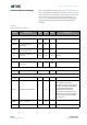
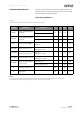
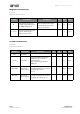
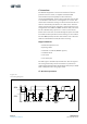
AS5600 − Absolute Maximum Ratings
Stresses beyond those listed under Absolute Maximum Ratings
may cause permanent damage to the device. These are stress
ratings only. Functional operation of the device at these or any
other conditions beyond those indicated under Operating
Conditions is not implied. Exposure to absolute maximum
rating conditions for extended periods may affect device
reliability.
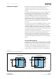
Figure 5:
Absolute Maximum Ratings
Symbol Parameter Min Max Units Comments
Electrical Parameters
VDD5V
DC Supply Voltage at VDD5V
pin
-0.3 6.1 V
VDD3V3
DC Supply Voltage at
VDD3V3 pin
-0.3 4.0 V
VIO
DC Supply Voltage at all
digital or analog pins
-0.3 VDD+0.3 V
I
SCR
Input current (latch-up
immunity)
-100 100 mA JESD78
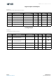
Continuous Power Dissipation (T
A
= 70°C)
P
T
Continuous power
dissipation
50 mW
Electrostatic Discharge
ESD
HBM
Electrostatic discharge HBM ±1 kV MIL 883 E method 3015.7
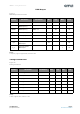
Temperature Ranges and Storage Conditions
T
STRG
Storage temperature range -55 125 °C
T
BODY
Package body temperature 260 °C
ICP/JEDEC J-STD-020
The reflow peak soldering
temperature (body temperature) is
specified according to IPC/JEDEC
J-STD-020 “Moisture/Reflow
Sensitivity Classification for
Non-hermetic Solid State Surface
Mount Devices.” The lead finish for
Pb-free leaded packages is “Matte
Tin” (100% Sn)
RH
NC
Relative humidity
(non-condensing)
585 %
MSL Moisture sensitivity level 3 ICP/JEDEC J-STD-033
Absolute Maximum Ratings