
Data Sheet

Page 32 ams Datasheet
Document Feedback [v1-06] 2018-Jun-20
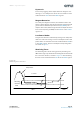
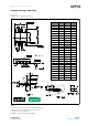
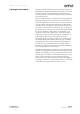
AS5600 − Application Information
Schematic
All required external components are shown below for the
reference application diagram. To improve EMC and for remote
applications, consider additional protection circuitry.
Figure 37:
Application Diagram for Angle Readout and Programming Through OUT Pin (Option B)
Note(s):
1. Consider that the output is driven high by an internal pull-up resistor during programming through the OUT pin. Disconnect
additional external load during the programming procedure.
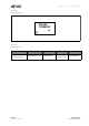
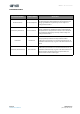
Figure 38:
Application Diagram for Angle Readout and Programming with I²C (Option A and Option C)
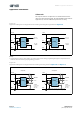
Application Information
GND -> CW
VDD -> CCW
PGO = GND
-> OptionB
4.5-5.5V
GND
AS5600
1 VDD5V
2 VDD3V3
3 OUT
4 GND
DIR 8
SCL 7
SDA 6
PGO 5
OUT
C1 C2
5V Operation
3-3.6V*
3.3V Operation
GND -> CW
VDD -> CCW
GND
AS5600
1 VDD5V
2 VDD3V3
3 OUT
4 GND
DIR 8
SCL 7
SDA 6
PGO 5
OUT
C1 C**
* Supply voltage for pe rmanent programming is 3.3–3.6V
** 10μF Capacitor required during permanent programming
PGO = GND
-> OptionB
GND -> CW
VDD -> CCW
To MCU
4.5-5.5V
GND
AS5600
1 VDD5V
2 VDD3V3
3 OUT
4 GND
DIR 8
SCL 7
SDA 6
PGO 5
OUT
R
PU
R
PU
C1 C2
5V Operation
3-3.6V*
3.3V Operation
GND -> CW
VDD -> CCW
To MCU
GND
AS5600
1 VDD5V
2 VDD3V3
3 OUT
4 GND
DIR 8
SCL 7
SDA 6
PGO 5
OUT
R
PU
R
PU
C1 C**
* Supply voltage for pe rmanent programming is 3.3–3.6V
** 10μF Capacitor required during permanent programming
-> OptionC
for Programming
with OUT Pin
PGO = GND
-> OptionC
for Programming
with OUT Pin
PGO = GND