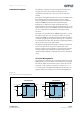
AS5600 12-Bit Programmable Contactless Potentiometer General Description The AS5600 is an easy to program magnetic rotary position sensor with a high-resolution 12-bit analog or PWM output. This contactless system measures the absolute angle of a diametric magnetized on-axis magnet. This AS5600 is designed for contactless potentiometer applications and its robust design eliminates the influence of any homogenous external stray magnetic fields.
AS5600 − General Description Benefits Features • Low-power consumption • Automatic entry into low-power mode • Easy setup • Automatic magnet detection • Small form factor • SOIC-8 package • Robust environmental tolerance • Wide temperature range: -40°C to 125°C Applications The AS5600 is ideally suited for contactless potentiometers, contactless knobs, pedals, RC servos and other angular position measurement solutions.
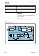
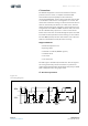
AS5600 − Pin Assignments Pin Assignments Figure 3: SOIC-8 Pin-Out 1 8 DIR VDD3V3 2 7 SCL OUT 3 6 SDA GND 4 5 PGO AS5600 VDD5V Figure 4: Pin Description Pin Number Name 1 VDD5V Supply Positive voltage supply in 5V mode (requires 100nF decoupling capacitor) 2 VDD3V3 Supply Positive voltage supply in 3.
AS5600 − Absolute Maximum Ratings Absolute Maximum Ratings Stresses beyond those listed under Absolute Maximum Ratings may cause permanent damage to the device. These are stress ratings only. Functional operation of the device at these or any other conditions beyond those indicated under Operating Conditions is not implied. Exposure to absolute maximum rating conditions for extended periods may affect device reliability.
AS5600 − Electrical Characteristics Electrical Characteristics All limits are guaranteed. The parameters with minimum and maximum values are guaranteed with production tests or SQC (Statistical Quality Control) methods. Operating Conditions Figure 6: System Electrical Characteristics and Temperature Range Symbol Parameter VDD5V Positive supply voltage in 5.0V mode VDD3V3 Positive supply voltage in 3.3V mode Conditions Min Typ Max Units 4.5 5.0 5.5 V 3.3V operation mode 3.0 3.3 3.
AS5600 − Electrical Characteristics Digital Inputs and Outputs Figure 7: Digital Input and Output Characteristics Symbol Parameter V_IH High-level input voltage V_IL Low-level input voltage Conditions Min Typ Max 0.7 × VDD Units V 0.3 × VDD VDD - 0.5 V V_OH High-level output voltage V V_OL Low-level output voltage 0.
AS5600 − Timing Characteristics PWM Output Figure 9: PWM Output Characteristics Symbol Parameter Conditions Min Typ Max Units PWMf1 PWM frequency (1) PWMF = 00 115 Hz PWMf2 PWM frequency (1) PWMF = 01 230 Hz PWMf3 PWM frequency (1) PWMF = 10 460 Hz PWMf4 PWM frequency (1) PWMF = 11 920 Hz PWM_DC PWM duty cycle PWM_SR PWM slew rate I_O Output current for PWM output C_L Capacitive load for PWM output Cload = 1nF 2.9 97.1 % 0.5 2 V/μs ±0.5 mA 1 nF Note(s): 1.
AS5600 − Magnetic Characteristics Magnetic Characteristics Figure 11: Magnetic Characteristics Symbol Parameter Conditions Min Max Units Bz Orthogonal magnetic field strength, regular output noise ON_SLOW and ON_FAST Required orthogonal component of the magnetic field strength measured at the die's surface along a circle of 1mm 30 90 mT Bz_ERROR Minimum required orthogonal magnetic field strength, Magnet detection level 8 mT Max Units System Characteristics Figure 12: System Specificatio
AS5600 − Detailed Description Detailed Description The AS5600 is a Hall-based rotary magnetic position sensor using planar sensors that convert the magnetic field component perpendicular to the surface of the chip into a voltage. The signals coming from the Hall sensors are first amplified and filtered before being converted by the analog-to-digital converter (ADC).
AS5600 − Detailed Description I²C Interface The AS5600 supports the 2-wire Fast-mode Plus I²C-slave protocol in device mode, in compliance with the NXP Semiconductors (formerly Philips Semiconductors) specification UM10204. A device that sends data onto the bus is a transmitter and a device receiving data is a receiver. The device that controls the message is called a master. The devices that are controlled by the master are called slaves.
AS5600 − Detailed Description I²C Electrical Specification Figure 15: I²C Electrical Specifications Symbol Parameter Conditions Min Typ Max Unit VIL Logic low input voltage -0.3 0.3 x VDD V VIH Logic high input voltage 0.7 x VDD VDD + 0.3 V VHYS Hysteresis of Schmitt trigger inputs VDD > 2.5V VOL Logic low output voltage (open-drain or open-collector) at 3 mA sink current VDD > 2.5V IOL Logic low output current VOL = 0.
AS5600 − Detailed Description I²C Timing Figure 16: I²C Timing Symbol Parameter Min Max Unit 1.0 MHz fSCLK SCL clock frequency tBUF Bus free time (time between the STOP and START conditions) 0.5 μs Hold time; (Repeated) START condition (1) 0.26 μs tLOW Low phase of SCL clock 0.5 μs tHIGH High phase of SCL clock 0.26 μs tSU;STA Setup time for a Repeated START condition 0.
AS5600 − Detailed Description I²C Modes Invalid Addresses There are two addresses used to access an AS5600 register. The first is the slave address used to select the AS5600. All I²C bus transactions include a slave address. The slave address of the AS5600 is 0x36 (0110110 in binary) The second address is a word address sent in the first byte transferred in a write transaction. The word address selects a register on the AS5600. The word address is loaded into the address pointer on the AS5600.
AS5600 − Detailed Description Accordingly, the following bus conditions have been defined: Bus Not Busy Both SDA and SCL remain high. Start Data Transfer A change in the state of SDA from high to low while SCL is high defines the START condition. Stop Data Transfer A change in the state of SDA from low to high while SCL is high defines the STOP condition. Data Valid The state of the data line represents valid data when, after a START condition, SDA is stable for the duration of the high phase of SCL.
AS5600 − Detailed Description Depending on the state of the R/W bit, two types of data transfer are possible: Data Transfer from a Master Transmitter to a Slave Receiver The first byte transmitted by the master is the slave address, followed by R/W = 0. Next follows a number of data bytes. The slave returns an acknowledge bit after each received byte. If the slave does not understand the command or data it sends a not acknowledge (NACK). Data is transferred with the most significant bit (MSB) first.
AS5600 − Detailed Description S Figure 18: Data Write (Slave Receiver Mode) 0110110 0 A XXXXXXXX A XXXXXXXX S – Start A – Acknowledge (ACK) P – Stop A XXXXXXXX A XXXXXXXX A P Data transferred: X+1 Bytes + Acknowledge Slave Transmitter Mode (Read Mode) The first byte is received and handled as in the slave receiver mode. However, in this mode, the direction bit indicates that the AS5600 will drive data on SDA.
AS5600 − Detailed Description 0110110 0 A XXXXXXXX S – Start Sr – Repeated Start A – Acknowledge (ACK) NA – Not Acknowledge (NACK) P – Stop A Sr S Figure 20: Data Read with Address Pointer Reload (Slave Transmitter Mode) 0110110 1 A XXXXXXXX A XXXXXXXX A XXXXXXXX NA P Data transferred: X+1 Bytes + Acknowledge Note: Last data byte is followed by NACK SDA and SCL Input Filters Input filters
AS5600 − Register Description Register Description The following registers are accessible over the serial I²C interface. The 7-bit device address of the slave is 0x36 (0110110 in binary). To permanently program a configuration, a non-volatile memory (OTP) is provided.
AS5600 − Register Description ZPOS/MPOS/MANG Registers These registers are used to configure the start position (ZPOS) and a stop position (MPOS) or maximum angle (MANG) for a narrower angular range. The angular range must be greater than 18 degrees. In case of narrowed angular range, the resolution is not scaled to narrowed range (e.g. 0° to 360°(full-turn) → 4096dec; 0° to180°→2048dec). To configure the angular range, see Angle Programming.
AS5600 − Register Description STATUS Register The STATUS register provides bits that indicate the current state of the AS5600.
AS5600 − Register Description Burn_Angle Command (ZPOS, MPOS) The host microcontroller can perform a permanent programming of ZPOS and MPOS with a BURN_ANGLE command. To perform a BURN_ANGLE command, write the value 0x80 into register 0xFF. The BURN_ANGLE command can be executed up to 3 times. ZMCO shows how many times ZPOS and MPOS have been permanently written. This command may only be executed if the presence of the magnet is detected (MD = 1).
AS5600 − Register Description There are three recommended methods for programming the angular range: • Option A: Angle Programming Through the I²C Interface • Option B: Angle Programming Through the OUT Pin • Option C: Programming a Maximum Angular Range Through the I²C Interface Figure 24: Option A: Angle Programming Through the I²C Interface Use the correct hardware configuration shown in Figure 37 and Figure 38. Step 1 Power up the AS5600. Step 2 Turn the magnet to the start position.
AS5600 − Register Description Figure 25: Option B: Angle Programming Through the OUT Pin Use the correct hardware configuration shown in Figure 37 and Figure 38. The PGO pin is connected to GND and the OUT pin is pulled high by an internal resistor until the programming procedure is finished. Step 1 Power up the AS5600. Step 2 Position the magnet in the start position. Step 3 Pull the OUT pin to GND for at least 100 ms, then allow the pin to float.
AS5600 − Register Description Figure 26: Option C: Programming a Maximum Angular Range Through the I²C Interface Use the correct hardware configuration shown in Figure 37 and Figure 38. Step 1 Power up the AS5600. Step 2 Use the I²C interface to write the maximum angular range into the MANG register. For example, if the maximum angular range is 90 degrees, write the MANG register with 0x400. Configure additional configuration settings by writing the CONFIG register. Wait at least 1 ms.
AS5600 − Register Description Analog Output Mode By default, the AS5600 output stage is configured as analog ratiometric output. The Digital to Analog Converter (DAC) has 12-bit resolution. In default mode, the lower reference voltage for the DAC is GND, while the upper reference voltage is VDD. The output voltage on the OUT pin is ratiometric between GND and VDD. The maximum angular range can be programmed from 18 degrees to 360 degrees. The default range is 360 degrees.
AS5600 − Register Description Figure 28: Output Characteristic Over a Range Smaller Than 360° Output Voltage AOUT[V] VDD 0 DEG λ θMAX Angle (DEG) λ 360 DEG If the maximum angular range is smaller than 360 degrees, the DAC resolution is automatically reduced. If θ max is the maximum angle, the number of steps N of the output signal OUT is: N = (θ max/360) × 4096 The AS5600 also allows selecting the output dynamic characteristics of the OUT signal with the OUTS bits in the CONF register.
AS5600 − Register Description PWM Output Mode The AS5600 output stage can be programmed in the OUTS bits of the CONF register for a PWM-encoded digital output (OUTS = 10). In this mode, the OUT pin provides a digital PWM signal. The duty cycle of each pulse is proportional to the absolute angle of the rotating magnet. The PWM signal consists of a frame of 4351 PWM clock periods as shown in Figure 30.
AS5600 − Register Description Step Response and Filter Settings The AS5600 has a digital post-processing programmable filter which can be set in fast or slow modes. The fast filter mode can be enabled by setting a fast filter threshold in the FTH bits of the CONF register. If the fast filter is OFF, the step output response is controlled by the slow linear filter. The step response of the slow filter is programmable with the SF bits in the CONF register.
AS5600 − Register Description For a fast step response and low noise after settling, the fast filter can be enabled. The fast filter works only if the input variation is greater than the fast filter threshold, otherwise the output response is determined only by the slow filter. The fast filter threshold is programmed with the FTH bits in the CONF Register.
AS5600 − Register Description Figure 34: Step Response (fast filter ON) Noise Fast Filter Noise slow filter Input Output response Threshold Sampling Frequency Fast filter step response Settling Time according slow filter setting Direction (clockwise vs. counterclockwise) The AS5600 allows controlling the direction of the magnet rotation with the DIR pin. If DIR is connected to GND (DIR = 0) a clockwise rotation viewed from the top will generate an increment of the calculated angle.
AS5600 − Register Description Hysteresis To avoid any toggling of the output when the magnet is not moving, a 1 to 3 LSB hysteresis of the 12-bit resolution can be enabled with the HYST bits in the CONF register. Magnet Detection As a safety and diagnostic feature, the AS5600 indicates the absence of the magnet.
AS5600 − Application Information Application Information Schematic All required external components are shown below for the reference application diagram. To improve EMC and for remote applications, consider additional protection circuitry. Figure 37: Application Diagram for Angle Readout and Programming Through OUT Pin (Option B) 5V Operation 3.3V Operation 4.5-5.5V 3-3.
AS5600 − Application Information Figure 39: Recommended External Components Component Symbol Value Units Notes VDD5V buffer capacitor C1 100 nF 20% LDO regulator capacitor C2 1 μF 20%; < 100 mΩ; Low ESR ceramic capacitor Optional pull-up for I²C bus RPU 4.7 KΩ Refer to UM10204 for RPU sizing Note(s): 1.
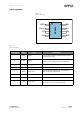
AS5600 − Application Information Mechanical Data The internal Hall elements are placed in the center of the package on a circle with a radius of 1 mm. Figure 41: Hall Element Positions Note(s): 1. All dimensions in mm. 2. Die thickness 356μm nom.
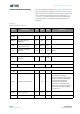
AS5600 − Package Drawings & Markings Package Drawings & Markings Figure 42: SOIC8 Package Outline Drawing Symbol Nom Max A - - 1.75 A1 0.10 - 0.25 A2 1.25 - - b 0.31 - 0.51 c 0.17 - 0.25 D - 4.90 BSC - E - 6.00 BSC - E1 - 3.90 BSC - e - 1.27 BSC - L 0.40 - 1.27 L1 - 1.04 REF - L2 - 0.25 BSC - R 0.07 - - R1 0.07 - - h 0.25 - 0.50 Θ 0º - 8º Θ1 5º - 15º Θ2 0º - - aaa - 0.10 - bbb - 0.20 - ccc - 0.10 - ddd - 0.
AS5600 − Package Drawings & Mark ings Figure 43: Package Marking AS5600 YYWWRZZ @ Figure 44: Packaging Code YY Last two digits of the manufacturing year Page 36 Document Feedback WW Manufacturing week R Plant identifier ZZ @ Free choice/ traceability code Sublot identifier ams Datasheet [v1-06] 2018-Jun-20
AS5600 − Ordering & Contact Information Ordering & Contact Information Figure 45: Ordering Information Ordering Code Package Marking Delivery Form Delivery Quantity AS5600-ASOT SOIC-8 AS5600 13” Tape&Reel in dry pack 2500 pcs AS5600-ASOM SOIC-8 AS5600 7” Tape&Reel in dry pack 500 pcs Buy our products or get free samples online at: www.ams.com/Products Technical Support is available at: www.ams.com/Technical-Support Provide feedback about this document at: www.ams.
AS5600 − RoHS Compliant & ams Green Statement RoHS Compliant & ams Green Statement RoHS: The term RoHS compliant means that ams AG products fully comply with current RoHS directives. Our semiconductor products do not contain any chemicals for all 6 substance categories, including the requirement that lead not exceed 0.1% by weight in homogeneous materials. Where designed to be soldered at high temperatures, RoHS compliant products are suitable for use in specified lead-free processes.
AS5600 − Copyrights & Disclaimer Copyrights & Disclaimer Copyright ams AG, Tobelbader Strasse 30, 8141 Premstaetten, Austria-Europe. Trademarks Registered. All rights reserved. The material herein may not be reproduced, adapted, merged, translated, stored, or used without the prior written consent of the copyright owner. Devices sold by ams AG are covered by the warranty and patent indemnification provisions appearing in its General Terms of Trade.
AS5600 − Document Status Document Status Document Status Product Preview Preliminary Datasheet Datasheet Datasheet (discontinued) Page 40 Document Feedback Product Status Definition Pre-Development Information in this datasheet is based on product ideas in the planning phase of development.
AS5600 − Revision Information Revision Information Changes from 1-05 (2018-May-18) to current revision 1-06 (2018-Jun-20) Page Updated Figure 6 5 Updated text under ZPOS/MPOS/MANG Registers 19 Note(s): 1. Page and figure numbers for the previous version may differ from page and figure numbers in the current revision. 2. Correction of typographical errors is not explicitly mentioned.
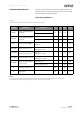
AS5600 − Content Guide Content Guide 1 1 2 2 General Description Key Benefits & Features Applications Block Diagram 3 4 Pin Assignments Absolute Maximum Ratings 5 5 6 6 7 Electrical Characteristics Operating Conditions Digital Inputs and Outputs Analog Output PWM Output 7 8 8 Timing Characteristics Magnetic Characteristics System Characteristics 9 9 10 10 10 11 12 13 13 13 13 Detailed Description IC Power Management I²C Interface Supported Modes I²C Interface Operation I²C Electrical Specificatio
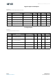
AS5600 − Content Guide ams Datasheet [v1-06] 2018-Jun-20 31 31 Low Power Modes Watchdog Timer 32 32 33 34 Application Information Schematic Magnetic Requirements Mechanical Data 35 37 38 39 40 41 Package Drawings & Markings Ordering & Contact Information RoHS Compliant & ams Green Statement Copyrights & Disclaimer Document Status Revision Information Page 43 Document Feedback