
Memory Card Specification Sheet

©Copyright 2000-2007 SD Card Association
SDIO Simplified Specification Version 2.00
36
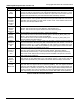
Field Type Description
Function
CSA
Enable
R/W This bit controls access to the Code Storage Area for this function. If this bit is cleared to
0, then any read or write access to the CSA shall be blocked. If this bit is set to 1, then
access to the CSA is allowed. This bit is cleared to 0 upon reset. If this function does not
support CSA (0xn00 bit 6=0), then this bit shall be R/O and always read as 0.
Extended
SDIO
Standard
Function
interface
code
R/O This is the extension of the SDIO Standard Function interface code. If the SDIO Standard
Function interface code is greater than 0xE, then this byte shall contain the code and the
standard code (0x100 bits 3-0) shall contain a value of 0xF. If the standard code is less
than 0xF, then this byte shall be 0x00.
SPS
(Support
Power
Selection)
R/O This bit indicates if the function has Power Selection.
SPS=0 :This function has no Power Selection. EPS shall be zero.
SPS=1 :This function has 2 power modes which are selected by EPS.
EPS
(Enable
Power
Selection)
R/W EPS=0(default): The function operates in Higher Current Mode
The maximum current for the function shall be given in TPLFE_HP_MAX_PWR_3.3V
EPS=1: The function works in Lower Current Mode
The maximum current for the function shall be given in TPLFE_LP_MAX_PWR_3.3V
This bit shall be reset when IOEx=0.
Address
pointer to
Function
CIS
R/O These three bytes make up a 24-bit pointer (only the lower 17 bits are used) to the start of
the Card Information Structure (CIS) that is associated with each function. The CIS is
defined in section 6.11. A CIS is mandatory for each function on an SDIO card. This
pointer is stored in little-endian format (LSB first). This register points to the End of Chain
tuple if the function is not supported on the card.
Address
pointer to
Function
CSA
R/W These three bytes make up a 24-bit pointer to the desired byte in the CSA to read or write.
After any read or write to the CSA access window register, this pointer shall be
automatically incremented by 1. If this function does not support CSA (0xn00 bit 6=0),
then these 24 bits shall be R/O and always read as 0x000000. This pointer is stored in
little-endian format (LSB first).
Data
access
window to
CSA
R/W Any read or write to this address when the CSA is enabled (0xn00 bit 7=1), shall pass
data to/from the byte addressed by the CSA address pointer. If this function does not
support CSA (0xn00 bit 6=0), then these 8 bits shall be R/O and always read as 0x00.
Function
1-7 I/O
Block Size
R/W This 16-bit register sets the block size for I/O block operations for each function (1-7). If
this card does not support I/O block operations (SMB=0), then this register becomes
read-only and shall always read 0x0000. The maximum block size is 2048 (0x0800) and
the minimum is 1 (0x0001). At power-up or reset, this register shall be initially loaded with
a value of 0x0000. The host is responsible for setting the appropriate value for the block
size supported by each function. This pointer is stored in little-endian format (LSB first).
Table 6-4 FBR bit and field definitions