
User manual


Appendix
ComTec GmbH 7-5
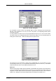
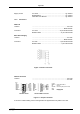
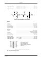
'GO' Line
Location: ............................................................................................. PCI card
.............................................................................. I/O port connector
.............................................................................................FMP bus
Connector: 2 pin header on PCI card: ............... LUMBERG 2,5 MSFW 2(MBX)
suitable socket connector: .............................LUMBERG 2,5 MBX 2
Line Type : ......................................................................open drain / wired-AND
Pull-Resistors: BASE: ............................................................................ 1kΩ to VCC
QUAD ADC PORT module: ........................................ 1MΩ to GND
PCI card: .................................................................... 4.7kΩ to VCC
Input HIGH voltage: ............................................................................................ min. 2.0V
Input LOW voltage: ........................................................................................... max. 0.8V
Output LOW voltage: I
OutLOW
= 15mA .................................................................. max. 0.8V
FMP Bus
Location: .............................................................................any MPA-3 module
Connector: ............................................................... 50 pin female CENTRONIX
Module's Power Supply
Location: .............................................................................any MPA-3 module
Connector: BASE power output ........................................... 9 pin female D-SUB
Quad ADC Port module power input.................... 9 pin male D-SUB
AUX 1 & 2
Location: .....................................................................................BASE module
Connector: ........................................................................................female BNC
Input HIGH voltage: (at AUX
i
I/O, ref. Figure 7.6)
7
............................................ min. 2.0V
Input LOW voltage: (at AUX
i
I/O,) .................................................................... max. 0.8V
7
Note: input and output voltages are measured at the internal logic pads not at the external connectors. Thus, the corresponding
pull and series resistors must be considered to get the external voltages
BASE module
Quad ADC
Port module MPA-3 PCI card
GO LI NE
1M0
22R
GO I N
VCC
1k0
22R
/ GO OUT GO IN
VCC
VCC
Quad ADC
Port module
1M0
22R
GO IN
VCC
4k7
22R
/ GO OUT GO I N
VCC
Figure 7.5: GO Line circuit schematic