
Integration Guide

3 of 6
O5K-SCR2_Integration_Guide - 000104.doc
1 The Module
Product Marketing Name: Smartcard Reader 2.0
HVIN: 03740300
FVIN: 07337130
FCC ID: O5K-SCR2
IC: 8312A-SCR2
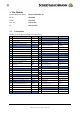
1.1 Connections
Pinning of the 52 pin PCIe Edge Connector (ST1)
PIN
Description
Netlabel
PIN
Description
Netlabel
1
Trace Clock (Trace Debug Port)
Trace_CLK
27
Ground
GND
2
3.3 V DC Input
+3V3
28
+5V Input (buffered by GoldCap)
+5V_RTC_BATT
3
Trace Data 0 (Trace Debug Port)
Trace_D0
29
Ground
GND
4
Ground
GND
30
Universal I²C Bus Clock
TWCK2
5
Trace Data 1 (Trace Debug Port)
Trace_D1
31
SAM4 ISO 7816 I/O
IO4
6
+5 V DC Input
+5V
32
Universal I²C Bus Data
TWD2
7
Trace Data 2 (Trace Debug Port)
Trace_D2
33
JTAGSEL
JTAGSEL
8
SAM 3 card supply
VCC3
34
Ground
GND
9
Ground
GND
35
Ground
GND
10
SAM3 ISO 7816 I/O
IO3
36
USB signal D-
USB_DATA_N
11
Trace Data 3 (Trace Debug Port)
TRACE_D3
37
Ground
GND
12
SAM3 ISO 7816 CLK
CLK3
38
USB signal D+
USB_DATA_P
13
JTAG TST
TST
39
5V DC supply input
+5V
14
SAM3 ISO 7816 RESET
RST3
40
Ground
GND
15
Ground
GND
41
3.3 V DC supply input
+3V3
16
PD0 ATSAME70 JTAG Compliance Pin
PD0
42
Digital I/O to control a piezo buzzer
BUZZER
17
VBUS Detect
VBUS
43
Ground
GND
18
Ground
GND
44
RXD UART0
Boot_TTL_RXD
19
SAM4 card supply
VCC4
45
JTAG TDI
TDI
20
ERASE Input (reinitialising of Flash)
ERASE
46
TXD UART0
Boot_TTL_TXD
21
Ground
GND
47
JTAG TMS
TMS
22
Reset ATSAME70 (Active-low)
NRST
48
5V DC supply input
+5V
23
SAM4 ISO 7816 RESET
RST4
49
JTAG TCK
TCK
24
3.3 V DC supply input
+3V3
50
Ground
GND
25
SAM4 ISO 7816 CLK
CLK4
51
JTAG TDO
TDO
26
Ground
GND
52
3.3V DC supply input
+3V3