
Specifications


HW400p/M Technical Reference - 1.0, March 6, 2002 Panels 27
Flash ROM There are two types of Flash ROM on the HW400p/M:
• Two contiguous 512-kByte banks for the Boot PROM. U66 is the lower
bank while U65 is the upper bank. U66 is accessed by the MPC8245
upon power up or reset.
• An optional 0/2/4/8 Mbytes of high-density Flash, comprised of two Intel
3V Advance+ Boot Block Flash devices organized as 0/512KB/1MB/2MB
x 16 bits.
CPLD The Main CPLD generates chip selects, control signals, and read/write signals
for the devices on the I/O Bus based on the address and control signals from
the MPC8245. The CPLD’s internal registers also reside on the I/O Bus and
are accessible by the MPC8245. See Section 4-7, I/O Bus Control and
Miscellaneous Logic, for register details.
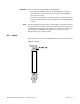
4-6. Panels
Figure 4-4 shows an example of the HW400p/M I/O panel for the main board.
Figure 4-4 I/O panel
S
BE