
User Manual


SPI Protocol Definition
5-6 TriFlash with SD Interface Product Manual (Preliminary), Rev. 1.2 © 2002/2003 SANDISK CORPORATION
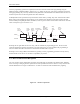
• The host is allowed to shut down the clock of a “busy” device. The TriFlash will complete the
programming operation regardless of the host clock. However, the host must provide a clock edge for
the device to turn off its busy signal. Without a clock edge, the TriFlash (unless previously
disconnected by de-asserting the CS signal) will force the dataOut line down, permanently.
5.1.9. Error Conditions
The following sections provide valuable information for TriFlash error conditions.
5.1.9.1. CRC and Illegal Commands
Unlike the SD Bus protocol, in SPI mode the device will always respond to a command. The response indicates
acceptance or rejection of the command. A command may be rejected in any one of the following cases:
• It is sent while the device is in read operation (except CMD12 which is legal).
• It is sent while the device is in Busy.
• Device is locked and it is other than Class 0 or 7 commands.
• It is not supported (illegal opcode).
• CRC check failed.
• It contains an illegal operand.
• It was out of sequence during an erase sequence.
NOTE: In case the host sends command while the device sends data in read operation then the response with an
illegal command indication may disturb the data transfer.
5.1.9.2. Read, Write and Erase Time-out Conditions
The times after which a time-out condition for read operations occur are (device independent) either 100 times
longer than the typical access times for these operations given below or 100ms. The times after which a time-out
condition for Write/Erase operations occur are (device independent) either 100 times longer than the typical
program times for these operations given below or 250ms. A device shall complete the command within this time
period, or give up and return an error message. If the host does not get any response with the given time-out it
should assume the device is not going to respond anymore and try to recover (e.g., reset the device, power cycle,
reject). The typical access and program times are defined as follows:
• Read—The read access time is defined as the sum of the two times given by the CSD parameters
TAAC and NSAC. These device parameters define the typical delay between the end bit of the read
command and the start bit of the data block.
• Write—The R2W_FACTOR field in the CSD is used to calculate the typical block program time
obtained by multiplying the read access time by this factor. It applies to all write/erase commands
(e.g., SET (CLEAR)_WRITE_PROTECT, PROGRAM_CSD (CID) and the block write commands).
• Erase—The duration of an erase command will be (order of magnitude) the number of write blocks
(WRITE_BL) to be erased multiplied by the block write delay.
5.1.10. Memory Array Partitioning
Same as for SD Bus mode.