
User Manual


SPI Protocol Definition
TriFlash with SD Interface Product Manual (Preliminary), Rev. 1.2 © 2002/2003 SANDISK CORPORATION
5-5
5.1.6. Read CID/CSD Registers
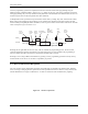
Unlike the SD Bus protocol (where the register contents are sent as a command response), reading the contents of
the CSD and CID registers in SPI mode is a simple read-block transaction. The device will respond with a standard
response token followed by a data block of 16 bytes suffixed with a 16-bit CRC.
The data time-out for the CSD command cannot be set to the device TAAC since this value is stored in the CSD.
Therefore, the standard response time-out value (N
CR
) is used for read latency of the CSD register.
5.1.7. Reset Sequence
The TriFlash requires a defined reset sequence. After power on reset or CMD0 (software reset), the device enters an
idle state. At this state, the only legal host commands are CMD1 (SEND_OP_COND), ACMD41
(SD_SEND_OP_COND), CMD59 (CRC_ON_OFF) and CMD58 (READ_OCR).
The host must poll the device (by repeatedly sending CMD1) until the ‘in-idle-state’ bit in the device response
indicates (by being set to 0) that the device completed its initialization processes and is ready for the next command.
In SPI mode, however, CMD1 has no operands and does not return the contents of the OCR register. Instead, the
host can use CMD58 (SPI Mode Only) to read the OCR register. It is the responsibility of the host to refrain from
accessing devices that do not support its voltage range.
The use of CMD58 is not restricted to the initialization phase only, but can be issued at any time. The host must poll
the device (by repeatedly sending CMD1) until the ‘in-idle-state’ bit in the device response indicates (by being set
to 0) that the device has completed its initialization process and is ready for the next command.
5.1.8. Clock Control
The SPI bus clock signal can be used by the SPI host to set the devices to energy-saving mode or to control the data
flow (to avoid under-run or over-run conditions) on the bus. The host is allowed to change the clock frequency or
shut it down.
There are a few restrictions the SPI host must follow:
• The bus frequency can be changed at any time (under the restrictions of maximum data transfer
frequency, defined by the TriFlash devices).
• It is an obvious requirement that the clock must be running for the TriFlash to output data or response
tokens. After the last SPI bus transaction, the host is required to provide 8 (eight) clock cycles for the
device to complete the operation before shutting down the clock. Throughout this 8-clock period, the
state of the CS signal is irrelevant. It can be asserted or de-asserted. Following is a list of the various
SPI bus transactions:
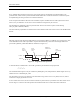
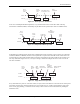
− A command/response sequence. Eight clocks after the device response end bit. The CS signal can
be asserted or de-asserted during these 8 clocks.
− A read data transaction. Eight clocks after the end bit of the last data block.
− A write data transaction. Eight clocks after the CRC status token.