
User Manual

Secure Digital (SD) Bus Protocol Description
TriFlash with SD Interface Product Manual (Preliminary), Rev. 1.2 © 2002/2003 SANDISK CORPORATION
4-29
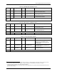
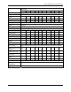
CMD S T content CRC E Z Z
P * * *
P S T content CRC E
<-------N
AC
cycles------->
<-Read Data->
DAT Z Z Z * * * * Z Z Z Z Z Z P * * * * * * * * P S D D D * * *
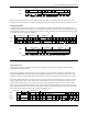
Figure 4-17. Timing of Single Block Read
Data transmission from the device starts after the access time delay N
AC
beginning from the end bit of the read
command. After the last data bit, the CRC check bits are suffixed to allow the host to check for transmission errors.
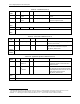
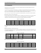
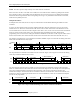
Multiple Block Read
In multiple block read mode, the device sends a continuous flow of data blocks following the initial host read
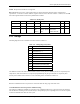
command. The data flow is terminated by a stop transmission command (CMD12). Figure 4-18 describes the timing
of the data blocks and Figure 4-19 describes the response to a stop command. The data transmission stops two clock
cycles after the end bit of the stop command.
<--Host command-->
<-N
CR
cycles->
<----Response---->
CMD S T content CRC E Z Z
P *
P S T content CRC E Z Z P P P P P P P P P P P P P
<---N
AC
cycles--->
<--Read Data-->
<-N
AC
cycles-> <-Read Data->
DAT Z Z Z * * * Z Z Z Z Z Z P * * * * * * P S content CRC E P * * * * * * P S D D D D D
Figure 4-18. Timing of Multiple Block Read Command
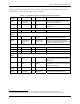
<–Host command–>
<–N
CR
cycles–>
<–Response–>
CMD S T content CRC E Z Z
P * * *
P S T content CRC E
DAT D D D * * * * * * * D D D E Z Z * * * * * * * * * * * * * * * * * *
Figure 4-19. Timing of Stop Command (CMD12, Data Transfer Mode)
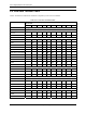
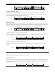
4.11.3. Data Write
Single Block Write
The host selects one device for data write operation by CMD7. The host sets the valid block length for block-
oriented data transfer by CMD16.
The basic bus timing for a write operation is given in Figure 4-20. The sequence starts with a single block write
command (CMD24) that determines (in the argument field) the start address. It is responded by the device on the
CMD line as usual. The data transfer from the host starts N
WR
clock cycles after the device response was received.
The data is suffixed with CRC check bits to allow the device to check it for transmission errors. The device sends
back the CRC check result as a CRC status token on the DAT0 line. In the case of transmission error the device
sends a negative CRC status (‘101’). In the case of non-erroneous transmission the device sends a positive CRC
status (‘010’) and starts the data programming procedure. When a flash programming error occurs the device will
ignore all further data blocks. In this case no CRC response will be sent to the host and, therefore, there will not be
CRC start bit on the bus and the three CRC status bits will read (‘111‘).
<-Host cmnd-> <-N
CR
->
<-Card response->
CMD E Z Z P * P S T Content CRC E Z Z P * * * * * * * * * * * * * * * * P P P P P P P P
<-N
WR
->
<-Write data->
CRC status <-Busy->
DAT0 Z Z
* * * * * *
Z Z Z * * * Z Z Z Z
P * P
S content CRC E
Z
Z S Status E S L*L E Z
DAT1-3 Z Z
* * * * * *
Z Z Z * * * Z Z Z Z
P * P
S content CRC E
Z
Z X X X X X X X X X Z
Figure 4-20. Timing of the Block Write Command