
User Manual

Secure Digital (SD) Bus Protocol Description
TriFlash with SD Interface Product Manual (Preliminary), Rev. 1.2 © 2002/2003 SANDISK CORPORATION
4-27
NOTE: Responses R4 and R5 are not supported.
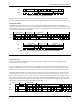
R6 (Published RCA response): code length 48 bits. The bits 45:40 indicate the index of the command to be
responded to—in that case it will be ‘000011’ (together with bit 5 in the status bits it means = CMD3). The 16 MSB
bits of the argument field are used for the published RCA number.
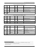
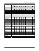
Table 4-16. R6 Response
Bit Position 47 46 [45:40] [39:8] Argument Field [7:1] 0
Width (bits) 1 1 6 16 16 7 1
Value ‘0’ ‘0’ x x x x ‘1’
Description Start bit Transmission bit Command
index
(‘000011’)
New published
RCA [31:16] of the
card
[15:0] card status bits:
23,22,19,12:0
(refer to Table 3-28)
CRC7 End bit
4.11. Timings
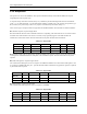
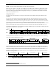
All timing diagrams use the schematics and abbreviations in Table 4-17.
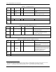
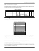
Table 4-17. Timing Diagram Symbols
S Start Bit (= 0)
T Transmitter Bit (Host = 1, Device = 0)
P One-cycle Pull-up (= 1)
E End Bit (=1)
Z High Impedance State (-> = 1)
D Data Bits
X Do not care Data Bits (from Device)
* Repeater
CRC Cyclic Redundancy Check Bits (7 Bits)
Device Active
Host Active
The difference between the P-bit and Z-bit is that a P-bit is actively driven to HIGH by the device respectively host
output driver, while Z-bit is driven to (respectively kept) HIGH by the pull-up resistors R
CMD
respectively R
DAT
.
Actively-driven P-bits are less sensitive to noise. All timing values are defined in Table 4-18.
4.11.1. Command and Response
Both host command and device responses are clocked out with the rising edge of the host clock.
Card identification and card operation conditions timing
The timing for CMD2 and ACMD41 is given below. The command is followed by a period of two Z bits (allowing
time for direction switching on the bus) and then by P bits pushed up by the responding device. The device response
to the host command starts after N
ID
clock cycles.