
User Manual


Secure Digital (SD) Bus Protocol Description
4-8 TriFlash with SD Interface Product Manual (Preliminary), Rev. 1.2 © 2002/2003 SANDISK CORPORATION
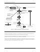
4.3.3. Device Identification Process
The host starts the device identification process with the identification clock rate f
OD
(refer to Table 3-7). In
TriFlash, the CMD line output drives are push-pull drivers.
After the bus is activated, the host will request the devices to send their valid operation conditions (ACMD41
preceding with APP_CMD—CMD55 with RCA=0x0000). The response to ACMD41 is the operation condition
register of the device. The same command shall be send to all of the new devices in the system. Incompatible
devices are sent into Inactive State. The host then issues the command ALL_SEND_CID (CMD2) to each device to
get its unique card identification (CID) number. A device that is unidentified (i.e., which is in Ready State) sends its
CID number as the response (on the CMD line). After the CID was sent by the device, it goes into Identification
State. Thereafter, the host issues CMD3 (SEND_RELATIVE_ADDR) asking the device to publish a new relative
card address (RCA), which is shorter than CID and which will be used to address the device in the future data
transfer mode (typically with a higher clock rate than f
OD
). Once the RCA is received, the device state changes to
the Stand-by State. At this point, if the host wants the device to have another RCA number, it may ask the device to
publish a new number by sending another SEND_RELATIVE_ADDR command to the device. The last published
RCA is the actual RCA number of the device.
The host repeats the identification process, i.e., the cycles with CMD2 and CMD3 for each device in the system.
After all the SD-interface devices are initialized, the host will initialize the MultiMediaCards that are in the system
(if any), using the CMD2 and CMD3 as given in the MultiMediaCard spec. Note that in the SD system all the
devices are connected separately so each MultiMediaCard will be initialized individually.
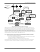
4.4. Data Transfer Mode
Until the content of all CSD registers is known by the host, the f
PP
clock rate must remain at f
OD
because some
devices may have operating frequency restrictions. The host issues SEND_CSD (CMD9) to obtain the Card
Specific Data (CSD register), e.g., block length, card storage capacity, maximum clock rate.