
User Manual

TriFlash Interface Description
TriFlash with SD Interface Product Manual (Preliminary), Rev. 1.2 © 2002/2003 SANDISK CORPORATION
3-21
3.5.4. SCR Register
In addition to the CSD register, there is another configuration register that is named SD CARD Configuration
Register (SCR). SCR provides information on the TriFlash device's special features that were configured into the
given device. The size of SCR register is 64 bit. This register shall be set in the factory by the TriFlash
manufacturer. The following table describes the SCR register content.
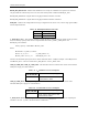
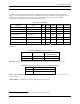
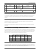
Table 3-23. SCR Fields
Description Field Width Cell Type SCR Slice SCR Value
9
SCR Code
SCR Structure SCR_STRUCTURE 4 R [63:60] Ver 1.0 0
SD Memory Card—Spec. Version SD_SPEC 4 R [59:56] Ver 1.0 0
data_status_after erases DATA_STAT_AFTER_ERASE 1 R [55:55] 0 0
SD Security Support SD_SECURITY 3 R [54:52] Prot 2
(Ver 1.0)
2
DAT Bus widths supported SD_BUS_WIDTHS 4 R [51:48] 1, 4 0101b
Reserved - 16 R [47:32] -
Reserved for manufacturer usage - 32 R [31:0] - 0
SCR_STRUCTURE—Version number of the related SCR structure in the SD Memory Card Physical Layer
Specification.
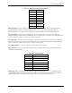
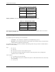
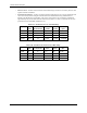
Table 3-24. SCR Register Structure Version
CSD_STRUCTURE CSD structure version Valid for SD Physical Layer
Specification Version
0 SCR version No. 1.0 Version 1.0-1.01
1-15 Reserved
SD_SPEC—Describes the SD Memory Card Physical Layer Specification version supported by this card.
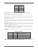
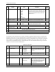
Table 3-25. SD Memory Card Physical Layer Specification Version
SPEC_VERS Physical Layer Specification Version Number
0 Version 1.0-1.01
1-15 Reserved
DATA_STAT_AFTER_ERASE—Defines the data status after erase, whether it is ‘0’ or ‘1’ (the status is card
vendor dependent).
SD_SECURITY—Describes the security algorithm supported by the device.
9
SCR (31:0) values might be changed because of this product’s internal improvement.