
User Manual

TriFlash Interface Description
TriFlash with SD Interface Product Manual (Preliminary), Rev. 1.2 © 2002/2003 SANDISK CORPORATION
3-15
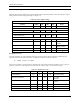
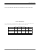
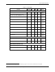
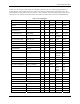
In Table 3-10, the cell type column defines the CSD field as Read only (R), One Time Programmable (R/W) or
erasable (R/W/E). For each field, the value in “real world” units and coded according to the CSD structure. The
Model dependent column marks (with a check mark—√) the CSD fields, which are model dependent. Note that the
CSD register in the TriFlash with the SD interface has a different structure than the CSD in the MultiMediaCard.
Table 3-10. CSD Register
Name Field Width Cell Type CSD-Slice CSD Value CSD Code
CSD structure CSD_STRUCTURE 2 R [127:126] 1.0 00b
Reserved - 6 R [125:120] - 000000b
data read access-time-1 TAAC 8 R [119:112] 1.5mS 00100110b
data read access-time-2 in CLK
cycles (NSAC*100)
NSAC 8 R [111:104] 0 00000000b
max. data transfer rate TRAN_SPEED 8 R [103:96] 25MHz 00110010b
card command classes CCC 12 R [95:84] All (include WP,
Lock/unlock)
1F5h
max. read data block length READ_BL_LEN 4 R [83:80] 512byte 1001b
partial blocks for read allowed READ_BL_PARTIAL 1 R [79:79] Yes 1b
write block misalignment WRITE_BLK_MISALIGN 1 R [78:78] No 0b
read block misalignment READ_BLK_MISALIGN 1 R [77:77] No 0b
DSR implemented DSR_IMP 1 R [76:76] No 0b
Reserved - 2 R [75:74] - 00b
device size C_SIZE 12 R [73:62] ST064=3919
ST032=1959
ST016=979
F4Fh
7A7h
3D3h
max. read current @VDD min VDD_R_CURR_MIN 3 R [61:59] 25mA 100b
max. read current @VDD max VDD_R_CURR_MAX 3 R [58:56] 25mA 011b
max. write current @VDD min VDD_W_CURR_MIN 3 R [55:53] 25mA 100b
max. write current @VDD max VDD_W_CURR_MAX 3 R [52:50] 35mA 100b
device size multiplier C_SIZE_MULT 3 R [49:47] ST128=3
ST064=3
ST032=3
ST016=3
011b
011b
011b
011b
erase single block enable ERASE_BLK_EN 1 R [46:46] Yes 1b
erase sector size SECTOR_SIZE 7 R [45:39] 32 blocks 0011111b
write protect group size WP_GRP_SIZE 7 R [38:32] 128 sectors 1111111b
write protect group enable WP_GRP_ENABLE 1 R [31:31] Yes 1b
Reserved for MultiMediaCard compatibility 2 R [30:29] - 00b
write speed factor R2W_FACTOR 3 R [28:26] X16 100b
max. write data block length WRITE_BL_LEN 4 R [25:22] 512byte 1001b
partial blocks for write allowed WRITE_BL_PARTIAL 1 R [21:21] No 0
Reserved - 5 R [20:16] - 00000b