
User Manual

TriFlash Interface Description
3-14 TriFlash with SD Interface Product Manual (Preliminary), Rev. 1.2 © 2002/2003 SANDISK CORPORATION
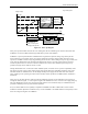
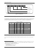
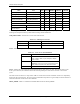
00h FFh 80h 00 00
24 16 8 7 4 3 0
Reserve
Operating
Voltage Range
2.7 to 3.6 volt
Reserved
Busy Bit
Figure 3-8. OCR Structure
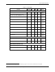
3.5.2. Card Identification (CID) Register
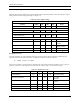
The CID register is 16 bytes long and contains a unique card identification number as shown in the table below. It is
programmed during device manufacturing and cannot be changed by TriFlash hosts. Note that the CID register in
the TriFlash with the SD interface has a different structure than the CID register in the MultiMediaCard.
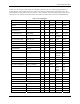
Table 3-9. CID Fields
Name Field Width (bits) CD-Slice CID Value
Manufacture ID MID 8 127:120 0x03
OEM/Application ID OID 16 119:104 SD ASCII Code 0x53, 0x44
Product Name PNM 40 103:64 ST128, ST064, ST032, ST016
Product Version
7
PRV 8 63:56 Product Revision (30)
Product Serial number PSN 32 55:24 Product serial number
Reserved 4 23:20
Manufacture date MDT 12 19:8 Manufacture date
CRC7 Checksum
8
CRC 7 7:1 CRC7
Not used always 1 1 0:0
3.5.3. CSD Register
The Card Specific Data (CSD) register contains configuration information required in order to access the device
data.
7
The product revision is composed of two Binary Coded Decimal (BCD) digits, four bits each, representing an “n.m” revision
number. The “n” is the most significant nibble and the “m” is the least significant nibble. Example: The PRV binary value
filed for product revision “6.2” will be: 0110 0010.
8
The CRC Checksum is computed by the following formula:
CRC Calculation: G(x)=x7+3+1
M(x)=(MID-MSB)*x119+...+(CIN-LSB)*x0
CRC[6...0]=Remainder[(M(x)*x7)/G(x)]