
User Manual
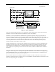

TriFlash Interface Description
TriFlash with SD Interface Product Manual (Preliminary), Rev. 1.2 © 2002/2003 SANDISK CORPORATION
3-13
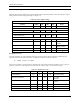
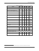
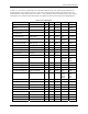
Table 3-8. OCR Register Definition
OCR Bit VDD Voltage Window
0-3 Reserved
4 1.6-1.7
5 1.7-1.8
6 1.8-1.9
7 1.9-2.0
8 2.0-2.1
9 2.1-2.2
10 2.2-2.3
11 2.3-2.4
12 2.4-2.5
13 2.5-2.6
14 2.6-2.7
15 2.7-2.8
16 2.8-2.9
17 2.9-3.0
18 3.0-3.1
19 3.1-3.2
20 3.2-3.3
21 3.3-3.4
22 3.4-3.5
23 3.5-3.6
24-30 Reserved
31 Card power up status bit (busy)
The level coding of the OCR register is as follows:
• Restricted voltage windows=LOW
• Card busy=LOW (bit 31)
The least significant 31 bits are constant and will be set as shown in Figure 3-8. If set, bit 32, the busy bit, informs
the host that the device power up procedure is finished.