
User Manual

TriFlash Interface Description
3-12 TriFlash with SD Interface Product Manual (Preliminary), Rev. 1.2 © 2002/2003 SANDISK CORPORATION
3.4.5. TriFlash-Specific Functions
The following sections list the TriFlash-specific functions.
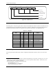
3.4.5.1. Ready/Busy Function [Output]
The RDY/BSY pin indicates ”0” if the TriFlash is in “Busy” condition. Busy condition is a period where the Data
paths of the TriFlash are not ready to get new data. The Busy condition, as defined in the SD Physical Specification,
may occur after or within the block transfer of any write or erase operations. After a host command is sent, the host
shall expect to get a Busy indication in any case that response of type R1b is expected. The RDY/BSY_B indication
is basically the same as the Busy indication that is indicated by DAT0 (as given in the SD/MMC Specs).
3.4.5.2. Write Protect Function [Input + Pullup]
This line shall be set to “0” (or maximum 10KOhm pull down resistor) in order to eliminate any write operations to
the TriFlash memory. An attempt to write to the TriFlash in that condition will set the WP_VIOLATION status bit
(bit [26] in the Card Status).
3.4.5.3. Reset Function [Input + Pullup]
If input is set to “0” (or maximum 10KOhm pull down resistor) it will force a Hardware RESET to the TriFlash.
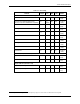
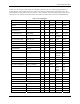
3.5. TriFlash Registers
There is a set of seven registers within the device interface. The OCR, CID, CSD and SCR registers carry the device
configuration information. The RCA register holds the device relative communication address for the current
session. The card status and SD status registers hold the communication protocol related status of the device.
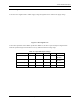
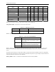
3.5.1. Operating Conditions Register (OCR)
The 32-bit operation conditions register stores the V
DD
voltage profile of the device. The TriFlash is capable of
executing the voltage recognition procedure (CMD1) with any standard TriFlash host using operating voltages form
2 to 3.6 Volts.
Accessing the data in the memory array, however, requires 2.7 to 3.6 Volts. The OCR shows the voltage range in
which the device data can be accessed. The structure of the OCR register is described in Table 3-8.