
User Manual
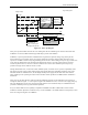

TriFlash Interface Description
3-10 TriFlash with SD Interface Product Manual (Preliminary), Rev. 1.2 © 2002/2003 SANDISK CORPORATION
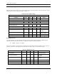
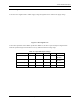
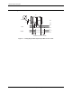
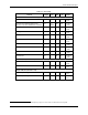
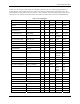
3.4.4. Bus Timing
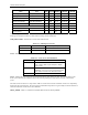
V
IH
V
IL
V
IH
V
IL
V
OH
V
OL
t
O DLY (max)
t
IH
Shaded areas are not valid.
Output
Clock
Input
t
O DLY
(min)
t
TLH
t
ISU
f
PP
t
WL
t
WH
t
THL
0.2
0.7
Figure 3-7. Timing Diagram Data Input/Output Referenced to Clock