
User Manual
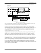

TriFlash Interface Description
TriFlash with SD Interface Product Manual (Preliminary), Rev. 1.2 © 2002/2003 SANDISK CORPORATION
3-9
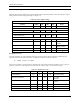
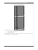
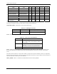
3.4.3. Bus Signal Levels
As the bus can be supplied with a variable supply voltage, all signal levels are related to the supply voltage.
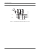
Figure 3-6. Bus Signal Levels
To meet the requirements of the JEDEC specification JESD8-1A, the device input and output voltages shall be
within the specified ranges listed in Table 3-6 for any VDD of the allowed voltage range.
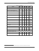
Table 3-6. Input and Output Voltages
Parameter Symbol Min. Max. Unit Conditions
Output HIGH voltage VOH
0.75∗VDD
V
IOH=-100 µA
@V
DD
(min.)
Output LOW voltage VOL
0.125∗VDD
V
IOL=100 µA
@V
DD
(min.)
Input HIGH voltage VIH
0.625∗VDD
VDD + 0.3 V
Input LOW voltage VIL VSS-0.3
0.25∗VDD
V