
User Manual

TriFlash Interface Description
3-8 TriFlash with SD Interface Product Manual (Preliminary), Rev. 1.2 © 2002/2003 SANDISK CORPORATION
3.4.2. Bus Operating Conditions
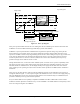
SPI Mode bus operating conditions are identical to SD mode bus operating conditions. The CS (chip select) signal
timing is identical to the input signal timing (see Figure 3-7).
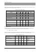
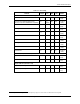
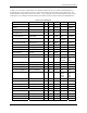
Table 3-4. Power Supply Voltage
General
Parameter Symbol Min. Max. Unit Remark
Peak voltage on all lines -0.3 VDD+0.3 V
All Inputs
Input Leakage Current -10 10
µA
All Outputs
Output Leakage Current -10 10
µA
Power Supply Voltage
Parameter Symbol Min. Max. Unit Remark
Supply Voltage V
DD
2.0 3.6 V CMD0, 15, 55, ACMD41
commands
Supply Voltage 2.7 3.6 V Except CMD0, 15, 55,
ACMD41 commands
Supply voltage differentials (V
SS1
, V
SS2
) -0.3 0.3 V
Power up Time 250 mS From 0V to V
DD
Min.
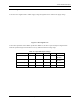
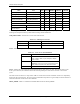
Bus Signal Line Load
The total capacitance CL of the CLK line of the bus is the sum of the bus master capacitance CHOST, the bus
capacitance CBUS itself and the capacitance CCARD of each device connected to this line:
CL = CHOST + CBUS + N∗CCARD
where N is the number of connected devices. Requiring the sum of the host and bus capacitances not to exceed 30
pF for up to 10 devices, and 40 pF for up to 30 devices, the values in Table 3-5 must not be exceeded.
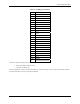
Table 3-5. Signal Line’s Load
Parameter Symbol Min. Max. Unit Remark
Pull-up resistance
R
CMD
R
DAT
10 100
kΩ
To prevent bus floating
Bus signal line capacitance C
L
250 pF f
PP
≤ 5 MHz,
21 devices
Bus signal line capacitance C
L
100 pF f
PP
≤ 25 MHz,
7 devices
Single card capacitance C
CARD
10 pF
Maximum signal line inductance 16 nH f
PP
≤ 25 MHz
Pull-up resistance inside device (pin 1) R
DAT3
10 90
kΩ
May be used for card detection