
User Manual

TriFlash with SD Interface Product Manual (Preliminary), Rev. 1.2 © 2002/2003 SANDISK CORPORATION
iii
Table of Contents
1. Introduction to the TriFlash with SD Interface .................................................................................................. 1-1
1.1. Scope................................................................................................................................................. 1-2
1.2. Product Models ................................................................................................................................. 1-2
1.3. System Features................................................................................................................................. 1-2
1.4. SD Memory Card Standard ............................................................................................................... 1-3
1.5. Functional Description ...................................................................................................................... 1-3
1.5.1. Flash Technology Independence............................................................................................. 1-4
1.5.2. Defect and Error Management................................................................................................ 1-4
1.5.3. Endurance ............................................................................................................................... 1-4
1.5.4. Wear Leveling......................................................................................................................... 1-4
1.5.5. Using the Erase Command...................................................................................................... 1-5
1.5.6. Automatic Sleep Mode............................................................................................................ 1-5
1.5.7. TriFlash—SD Bus Mode ........................................................................................................ 1-5
1.5.7.1. TriFlash Standard Compliance .............................................................................. 1-5
1.5.7.2. Negotiating Operation Conditions ......................................................................... 1-5
1.5.7.3. Device Acquisition and Identification ................................................................... 1-5
1.5.7.4. Device Status ......................................................................................................... 1-6
1.5.7.5. Memory Array Partitioning.................................................................................... 1-6
1.5.7.6. Read and Write Operations.................................................................................... 1-8
1.5.7.7. Data Transfer Rate................................................................................................. 1-9
1.5.7.8. Data Protection ...................................................................................................... 1-9
1.5.7.9. Erase ...................................................................................................................... 1-9
1.5.7.10. Write Protection................................................................................................... 1-9
1.5.7.11. Optional Copyright Protection............................................................................. 1-9
1.5.7.12. Copy Bit............................................................................................................... 1-10
1.5.7.13. The CSD Register ................................................................................................ 1-10
1.5.8. TriFlash—SPI Mode ............................................................................................................... 1-10
1.5.8.1. Negotiating Operating Conditions ......................................................................... 1-10
1.5.8.2. Card Acquisition and Identification....................................................................... 1-10
1.5.8.3. Card Status............................................................................................................. 1-10
1.5.8.4. Memory Array Partitioning.................................................................................... 1-10
1.5.8.5. Read and Write Operations.................................................................................... 1-11
1.5.8.6. Data Transfer Rate................................................................................................. 1-11
1.5.8.7. Data Protection in the TriFlash.............................................................................. 1-11
1.5.8.8. Erase ...................................................................................................................... 1-11
1.5.8.9. Write Protection..................................................................................................... 1-11
2. Product Specifications ........................................................................................................................................ 2-1
2.1. System Environmental Specifications............................................................................................... 2-1
2.2. Typical Power Requirements ............................................................................................................ 2-1
2.3. System Performance.......................................................................................................................... 2-2
2.4. System Reliability and Maintenance................................................................................................. 2-2
2.5. Physical Specifications...................................................................................................................... 2-3
3. TriFlash Interface Description............................................................................................................................ 3-1
3.1. General Description of Pins and Registers........................................................................................ 3-1
3.1.1. Pin Assignments in SD Bus Mode.......................................................................................... 3-1
3.1.2. Pin Assignments in SPI Mode................................................................................................. 3-2
3.1.3. Registers.................................................................................................................................. 3-2
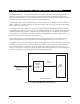
3.2. SD Bus Topology.............................................................................................................................. 3-3
3.3. SPI Bus Topology ............................................................................................................................. 3-5
3.4. Electrical Interface ............................................................................................................................ 3-6
3.4.1. Power-up ................................................................................................................................. 3-6