
User Manual

TriFlash Interface Description
3-2 TriFlash with SD Interface Product Manual (Preliminary), Rev. 1.2 © 2002/2003 SANDISK CORPORATION
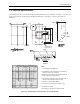
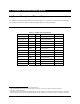
3.1.2. Pin Assignments in SPI Mode
Table 3-2. SPI Bus Mode Pad Definition
Pin # Name Type
4
Function Comment
H6, F1, C1, A2, A6 V
DD
S Supply Voltage
H7, H2, D1, B1, A7 V
SS
S Supply Voltage Ground
G2 DataOut I/O Device to Host Data and Status
G3 DAT1 I/O Unused Pull up to VDD
G6 DAT2 I/O Unused Pull up to VDD
G5 CS I Chip Select (Active low)
G1 CLK I Clock
G4 DataIn I Host to Device Commands and Data
B5 WPB I Write Protect (Active low)
G7 RSTB I Reset (Active low)
B2 RDY/BSY O Ready/Busy Interrupt
B3 SEL_A I Defines I/F Pull up to VDD
B4 SEL_B I Defines I/F Pull up to VDD
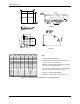
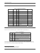
3.1.3. Registers
Each device has a set of information registers. A detailed description is given in Section 3.5.
Table 3-3. TriFlash Registers
Name Width Description
CID 128 Card identification number: individual card number for identification.
RCA
5
16 Relative card address: local system address of a device, dynamically
suggested by the device and approved by the host during initialization.
CSD 128 Card specific data: information about the device operation conditions.
SCR 64 SD Configuration Register: information about the TriFlash’s special
features capabilities.
OCR 32 Operation Condition Register.
The host may reset the devices by switching the power supply off and on again, or toggling the Reset pin. The
device has its own power-on detection circuitry, which puts the device into an idle state after the power-on. The
device can also be reset by sending the GO_IDLE (CMD0) command.
4
S=power supply; I=input; O=output using push-pull drivers.
5
The RCA register is not used (not available) in SPI Mode.