
User Manual

TriFlash with SD Interface Product Manual (Preliminary), Rev. 1.2 © 2002/2003 SANDISK CORPORATION
3-1
3. TriFlash Interface Description
3.1. General Description of Pins and Registers
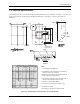
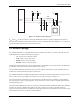
The TriFlash is a TFBGA package with 44 core balls (see Figure 2-3). The host is connected to the TriFlash using
the 11 interface connections shown on following 2 tables, plus power and ground balls.
3.1.1. Pin Assignments in SD Bus Mode
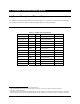
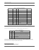
Table 3-1. SD Bus Mode Pad Definition
Pin # Name Type
1
Function Comment
H6, F1, C1, A2, A6 V
DD
S Supply Voltage
H7, H2, D1, B1, A7 V
SS
S Supply Voltage Ground
G2 DAT0 I/O Data Line [Bit 0]
G3 DAT1
2
I/O Data Line [Bit 1]
G6 DAT2 I/O Data Line [Bit 2]
G5 DAT3 I/O
3
Data Line [Bit 3]
G1 CLK I Clock
G4 CMD I/O Command/Response
B5 WPB I Write Protect (Active Low)
G7 RSTB I Reset (Active Low)
B2 RDY/BSY O Ready/Busy Interrupt
B3 SEL_A I Defines I/F Pull up to VDD
B4 SEL_B I Defines I/F Pull up to VDD
1
S=power supply; I=input; O=output using push-pull drivers.
2
The extended DAT lines (DAT1-DAT3) are inputs on power up. They start to operate as DAT lines after the
SET_BUS_WIDTH command.
3
After power up, this line is input with 50KOhm pull-up (can be used for device detection or SPI mode selection). The pull-up
should be disconnected by the user, during regular data transfer, with SET_CLR_CARD_DETECT (ACMD42) command.