
User Manual

SPI Protocol Definition
5-18 TriFlash with SD Interface Product Manual (Preliminary), Rev. 1.2 © 2002/2003 SANDISK CORPORATION
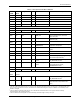
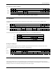
The device will resume busy signal (pulling DataOut low) one clock after the falling edge of CS.
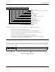
CS
H L * * * * * * * * * * * * * * * * * * * L L L L L L L L H H H L L L L
<-N
CS
-> <-N
WR
-> <-N
EC
-> <-N
DS
->
DataIN
X H H H Write Command H H H H H H H Data Block H H H H H H X X X H H H H
<-N
CR
->
DataOut
Z Z H H H * * * * * * * * H H H Card Resp H H H H H H H Data Resp Busy L Z Z Z Busy H
Figure 5-17. Data Write Operation
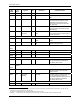
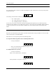
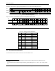
Figure 5-18 shows stop transmission operation in Multiple Block Write transfer.
CS L L L L L L L L L L L L L L L L L L L L L L H H H L L L L
<N
WR
-> <1byte-> <N
BR
-> <N
EC
-> <-N
DS
->
DataIn Data Block H H H H H H H H H Stop Tran
Token
H H H X X X H H H H
DataOut H H H H Data Resp Busy H H H H H H H H H Busy
12
L Z Z Z Busy H
Figure 5-18. Stop Transmission Operation
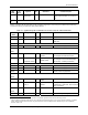
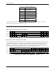
5.4.4. Timing Values
Table 5-5. Timing Constants Definitions
Min Max Unit
N
CS
0 - 8 Clock Cycles
N
CR
0 8 8 Clock Cycles
N
RC
1 - 8 Clock Cycles
N
AC
1 See footnote
13
8 Clock Cycles
N
WR
1 - 8 Clock Cycles
N
EC
0 - 8 Clock Cycles
N
DS
0 - 8 Clock Cycles
N
BR
0 1 8 Clock Cycles
N
CX
0 8 8 Clock Cycles
5.5. SPI Electrical Interface
The SPI Mode electrical interface is identical to that of the SD Bus mode.
12
The Busy may appear within N
BR
clocks after Stop Tran Token. If there is no Busy the host may continue to the next
command.
13
N
AC
maximum value shall be calculated using the following equation: MIN [([TAAC ∗ f + NSAC ∗ 100] ∗ 100/8), (100ms ∗
f/8)].