TriFlash with Secure Digital (SD) Interface Product Manual (Preliminary) CORPORATE HEADQUARTERS 140 Caspian Court Sunnyvale, CA 94089-1000 408-542-0500 FAX: 408-542-0503 URL: http://www.sandisk.
SanDisk® Corporation general policy does not recommend the use of its products in life support applications where in a failure or malfunction of the product may directly threaten life or injury. Per SanDisk Terms and Conditions of Sale, the user of SanDisk products in life support applications assumes all risk of such use and indemnifies SanDisk against all damages. The information in this manual is subject to change without notice.
Table of Contents 1. Introduction to the TriFlash with SD Interface .................................................................................................. 1-1 1.1. Scope ................................................................................................................................................. 1-2 1.2. Product Models ................................................................................................................................. 1-2 1.3. System Features......
Table of Contents 3.4.2. Bus Operating Conditions ....................................................................................................... 3-8 3.4.3. Bus Signal Levels.................................................................................................................... 3-9 3.4.4. Bus Timing.............................................................................................................................. 3-10 3.4.5. TriFlash-Specific Functions ........................
Table of Contents 5. SPI Protocol Definition ...................................................................................................................................... 5-1 5.1. SPI Bus Protocol ............................................................................................................................... 5-1 5.1.1. Mode Selection ....................................................................................................................... 5-1 5.1.2.
Table of Contents This page intentionally left blank. vi TriFlash with SD Interface Product Manual (Preliminary), Rev. 1.
1. Introduction to the TriFlash with SD Interface The SanDisk TriFlash is a very small, flash storage device, designed specifically for storage applications that put a premium on small form factor, low power and low cost. Flash is the ideal storage medium for portable, batterypowered devices. It features low power consumption and is non-volatile, requiring no power to maintain the stored data. It also has a wide operating range for temperature, shock and vibration.
Introduction to the TriFlash with SD Interface 1.1. Scope This document describes the key features and specifications of the TriFlash with SD interface, as well as the information required to interface this product to a host system. 1.2. Product Models The TriFlash is available in the capacities shown in Table 1-1. Table 1-1. TriFlash Capacities SD Model No. Capacities SDAT2FAH-128 128 Mb SDBT2FAH-256 256 Mb SDBT2FCH-512 512 Mb SDBT2FCH-1024 1024 Mb 1.3.
Introduction to the TriFlash with SD Interface The performance of the communication channel is described in Table 1-2. Table 1-2. SD Bus/SPI Bus Comparison TriFlash Using SD Bus TriFlash Using SPI Bus Six-wire communication channel (clock, command, 4 data lines). Three-wire serial data bus (Clock, dataIn, dataOut) + card specific CS signal (hardwired card selection). Error-protected data transfer. Optional non-protected data transfer mode available. Single or multiple block oriented data transfer.
Introduction to the TriFlash with SD Interface 1.5.1. Flash Technology Independence The 512-byte sector size of the TriFlash is the same as that in an IDE magnetic disk drive. To write or read a sector (or multiple sectors), the host computer software simply issues a Read or Write command to the TriFlash. This command contains the address. The host software then waits for the command to complete. The host software does not get involved in the details of how the flash memory is erased, programmed or read.
Introduction to the TriFlash with SD Interface 1.5.5. Using the Erase Command The Erase command provides the capability to substantially increase the write performance of the TriFlash. Once a sector has been erased using the Erase command, a write to that sector will be much faster. This is because a normal write operation includes a separate sector erase prior to write. 1.5.6.
Introduction to the TriFlash with SD Interface In addition, the TriFlash host can read the device’s CID register using the READ_CID command. The CID register is programmed during the TriFlash testing and formatting procedure, on the manufacturing floor. The TriFlash host can only read this register and not write to it. An internal pull-up resistor on the DAT3 line may be used for device detection (insertion/removal). The resistor can be disconnected during data transfer (using ACMD42). 1.5.7.4.
Introduction to the TriFlash with SD Interface TriFlash WP Group 0 Sector 1 Block 0 Block 1 Block 2 Block n Block 1 Block 2 Block n Sector 2 Sector 3 Sector n WP Group 1 WP Group n Protected Area (Copyright protection) Sector 1 Block 0 Sector n Figure 1-2. Memory Array Partitioning Table 1-3.
Introduction to the TriFlash with SD Interface 1.5.7.6. Read and Write Operations The TriFlash supports two read/write modes as shown in Figure 1-3.
Introduction to the TriFlash with SD Interface 1.5.7.7. Data Transfer Rate The TriFlash can be operated using either a single data line (DAT0) or four data lines (DAT0-DAT3) for data transfer. The maximum data transfer rate for a single data line is 25 Mb per second and for four data lines it is 100 Mb (12.5 MB) per second. 1.5.7.8. Data Protection Every sector is protected with an Error Correction Code (ECC).
Introduction to the TriFlash with SD Interface 1.5.7.12. Copy Bit The content of a TriFlash can be marked as an original or a copy using the copy bit in the CSD register. Once the Copy bit is set (marked as a copy) it cannot be cleared. The Copy bit of the TriFlash is programmed (during test and formatting on the manufacturing floor) as a copy. The TriFlash can be purchased with the copy bit set (copy) or cleared, indicating the TriFlash is a master.
Introduction to the TriFlash with SD Interface 1.5.8.5. Read and Write Operations In SPI mode, both single and multiple block data transfer modes are supported. 1.5.8.6. Data Transfer Rate In the SPI mode, only one data line is used for each direction. The SPI mode data transfer rate is the same as the SD Bus mode data transfer rate when using one data line only (up to 25Mbits per second). 1.5.8.7. Data Protection in the TriFlash Same as for the SD Bus mode. 1.5.8.8. Erase Same as in SD Bus mode. 1.5.
Introduction to the TriFlash with SD Interface This page intentionally left blank. 1-12 TriFlash with SD Interface Product Manual (Preliminary), Rev. 1.
2. Product Specifications For the specifications in the following sections, values are defined at ambient temperature and nominal supply voltage unless otherwise stated. 2.1. System Environmental Specifications Table 2-1. System Environmental Specifications Temperature Operating: -25° C to 85° C Non-Operating: -40° C to 85° C Humidity Operating: 8% to 95%, non-condensing Non-Operating: 8% to 95%, non-condensing ESD Protection ± 2kV, Human body model Vibration Operating: 15 G peak to peak max.
Product Specifications 2.3. System Performance Table 2-3. System Performance1 Typical Maximum Block Read Access Time 1.5 msec 100 msec CMD1 to Ready (after power up) 50 msec 100 msec Sleep to Ready 1 msec 2 msec 2.4. System Reliability and Maintenance Table 2-4.
Product Specifications 2.5. Physical Specifications The SanDisk TriFlash is a 44- and 56-pin Thin Fine-Pitched Ball Grid Array (TFBGA). See Figure 2-1 (56-pin) and Figure 2-2 (44-pin) for the physical specifications and dimensions. See Figure 2-3 for a top view of the pin definitions.
Product Specifications D A aaa A1 B Cavity A A1 E A2 bbb C Solder Ball C aaa ddd C Seating Plane (NOTE 2) DETAIL: A Oeee M C A B O fff M C "A" D1 B b H G F E D C B A E1 A (NOTE 3) e 1 (NOTE 6) "B" 12345678 Dimension in mm Symbol MIN NOM MAX A ----1.10 A1 0.32 0.35 0.38 A2 0.62 0.67 0.72 D 11.90 12.00 12.10 E 9.90 10.00 10.10 D1 --7.00 --E1 --7.00 --e --1.00 --b 0.40 0.45 0.50 aaa 0.10 bbb 0.10 ddd 0.15 eee 0.25 fff 0.10 MD/ME 8/8 Dimension in inch Min NOM MAX ----0.043 0.013 0.
Product Specifications H7 GND H6 VDD H5 DU G5 G6 DAT2 CSB_DAT3 H4 DU H3 DU H2 GND G4 CMD G3 DAT1 G2 DAT0 G1 CLK G8 DU G7 RSTB F8 DU F7 DU F2 DU F1 VDD E8 DU E7 DU E2 DU E1 DU D8 DU D7 DU D2 DU D1 GND C8 DU C7 DU C2 DU C1 VDD B8 DU B7 DU B6 DU B5 WPSB B4 SEL_B A7 GND A6 VDD A5 DU A4 DU B3 B2 SEL_A RDY/BSY A3 DU B1 GND A2 VDD NOTE: DU=Don't Use. Pin A1 ID Figure 2-3. TriFlash Pinout (Top View) TriFlash with SD Interface Product Manual (Preliminary), Rev. 1.
Product Specifications This page intentionally left blank. 2-6 TriFlash with SD Interface Product Manual (Preliminary), Rev. 1.
3. TriFlash Interface Description 3.1. General Description of Pins and Registers The TriFlash is a TFBGA package with 44 core balls (see Figure 2-3). The host is connected to the TriFlash using the 11 interface connections shown on following 2 tables, plus power and ground balls. 3.1.1. Pin Assignments in SD Bus Mode Table 3-1.
TriFlash Interface Description 3.1.2. Pin Assignments in SPI Mode Table 3-2.
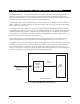
TriFlash Interface Description DAT2 CD/DAT3 CMD RDY/BSY VDD CLK RSTB WPB DAT0 DAT1 Interface Driver OCR[31:0] RCA[15:0] Card Interface Controller DSR[15:0] CSD[127:0] reset SCR[63:0] Memory Core Interface reset Power Connection CID[127:0] Memory Core Figure 3-1. TriFlash Architecture 3.2. SD Bus Topology The SD bus has six communication lines and three supply lines: • • • • • CMD—Command is a bi-directional signal. (Host and device drivers are operating in push pull mode.
TriFlash Interface Description Figure 3-2 shows the bus topology of several devices with one host in SD Bus mode. HOST CLK CLK Vdd Vss Vdd Vss D0-3(A), CMD(A) TriFlash (A) D0-D3, CMD CLK Vdd Vss D0-3(B), CMD(B) SD Memory Card (B) D0-D3, CMD CLK Vdd Vss D0-3(C) CMD(C) D0, CS, CMD MultiMediaCard (C) D1&D2 Not Connected Figure 3-2.
TriFlash Interface Description R DAT V SS R CM CMD DAT 0-3 TriFlash Host CLK C1 C 2 C3 Figure 3-3. SD Bus Circuitry Diagram RDAT and RCMD are pull-up resistors protecting the CMD and the DAT line against bus floating when all device drivers are in a hi-impedance mode. Refer to Table 3-5 for the component values and conditions. C1, C2 and C3 are the equivalent load capacitance (CL) of each line in the bus. 3.3.
TriFlash Interface Description Power Supply SPI Bus Master CS CS SPI Bus (CLK, DataIN, DataOut) TriFlash Card SPI Card Figure 3-4. SPI Bus System 3.4. Electrical Interface The following sections provide valuable information on TriFlash’s electrical interface. 3.4.1. Power-up The power up of the bus is handled locally in each TriFlash and in the bus master. 3-6 TriFlash with SD Interface Product Manual (Preliminary), Rev. 1.
TriFlash Interface Description Logic working level Supply voltage VDD max Valid voltage range for commands CMD0, 15, 55 and ACMD41. Bus master supply voltage Valid voltage range for all other commands and memory access. V DD min time Power up time Supply ramp up time Initialization sequence Initialization delay: The maximum of 1 msec, 74 clock cycles and supply ramp up time. Time out value for initialization process = 100 msec.
TriFlash Interface Description 3.4.2. Bus Operating Conditions SPI Mode bus operating conditions are identical to SD mode bus operating conditions. The CS (chip select) signal timing is identical to the input signal timing (see Figure 3-7). Table 3-4. Power Supply Voltage General Parameter Symbol Min. Max. Unit -0.3 VDD+0.3 V -10 10 µA -10 10 µA Symbol Min. Max. Unit Remark VDD 2.0 3.6 V CMD0, 15, 55, ACMD41 commands Supply Voltage 2.7 3.
TriFlash Interface Description 3.4.3. Bus Signal Levels As the bus can be supplied with a variable supply voltage, all signal levels are related to the supply voltage. Figure 3-6. Bus Signal Levels To meet the requirements of the JEDEC specification JESD8-1A, the device input and output voltages shall be within the specified ranges listed in Table 3-6 for any VDD of the allowed voltage range. Table 3-6.
TriFlash Interface Description 3.4.4. Bus Timing fPP 0.7 tWL tWH 0.2 Clock VIH tTLH tTHL tISU VIL tIH VIH Input VIL VOH Output tO DLY (max) tO DLY (min) VOL Shaded areas are not valid. Figure 3-7. Timing Diagram Data Input/Output Referenced to Clock 3-10 TriFlash with SD Interface Product Manual (Preliminary), Rev. 1.
TriFlash Interface Description Table 3-7. Bus Timing Parameter Symbol Min. Max. Unit Remark Clock CLK–All values are referred to min. (VIH) and max.
TriFlash Interface Description 3.4.5. TriFlash-Specific Functions The following sections list the TriFlash-specific functions. 3.4.5.1. Ready/Busy Function [Output] The RDY/BSY pin indicates ”0” if the TriFlash is in “Busy” condition. Busy condition is a period where the Data paths of the TriFlash are not ready to get new data. The Busy condition, as defined in the SD Physical Specification, may occur after or within the block transfer of any write or erase operations.
TriFlash Interface Description Table 3-8. OCR Register Definition OCR Bit VDD Voltage Window 0-3 Reserved 4 1.6-1.7 5 1.7-1.8 6 1.8-1.9 7 1.9-2.0 8 2.0-2.1 9 2.1-2.2 10 2.2-2.3 11 2.3-2.4 12 2.4-2.5 13 2.5-2.6 14 2.6-2.7 15 2.7-2.8 16 2.8-2.9 17 2.9-3.0 18 3.0-3.1 19 3.1-3.2 20 3.2-3.3 21 3.3-3.4 22 3.4-3.5 23 3.5-3.
TriFlash Interface Description 24 00h 16 8 7 FFh 80h 4 3 00 0 00 Reserve Operating Voltage Range 2.7 to 3.6 volt Reserved Busy Bit Figure 3-8. OCR Structure 3.5.2. Card Identification (CID) Register The CID register is 16 bytes long and contains a unique card identification number as shown in the table below. It is programmed during device manufacturing and cannot be changed by TriFlash hosts.
TriFlash Interface Description In Table 3-10, the cell type column defines the CSD field as Read only (R), One Time Programmable (R/W) or erasable (R/W/E). For each field, the value in “real world” units and coded according to the CSD structure. The Model dependent column marks (with a check mark—√) the CSD fields, which are model dependent. Note that the CSD register in the TriFlash with the SD interface has a different structure than the CSD in the MultiMediaCard. Table 3-10.
TriFlash Interface Description Name Field Width Cell Type CSD-Slice CSD Value CSD Code File format group FILE_FORMAT_GRP 1 R/W(1) [15:15] 0 0b copy flag (OTP) COPY 1 R/W(1) [14:14] Not Original 1b permanent write protection PERM_WRITE_PROTECT 1 R/W(1) [13:13] Not Protected 0b temporary write protection TMP_WRITE_PROTECT 1 R/W [12:12] Not Protected 0b File format FILE_FORMAT 2 R/W(1) [11:10] HD w/partition 00b 2 R/W [9:8] - 00b Reserved CRC CRC 7 R/W [7:1]
TriFlash Interface Description Table 3-13. Maximum Data Transfer Rate Definition TRAN_SPEED Bit Code 2:0 transfer rate unit: 0=100kbit/s, 1=1Mbit/s, 2=10Mbit/s, 3=100Mbit/s, 4... 7=Reserved 6:3 time value: 0=Reserved, 1=1.0, 2=1.2, 3=1.3, 4=1.5, 5=2.0, 6=2.5, 7=3.0, 8=3.5, 9=4.0, A=4.5, B=5.0, C=5.5, D=6.0, E=7.0, F=8.0 7 Reserved CCC—The TriFlash command set is divided into subsets (command classes). The card command class register CCC defines which command classes are supported by this device.
TriFlash Interface Description READ_BLK_MISALIGN—Defines if the data block to be read by one command can be spread over more than one physical block of the memory device. The size of the memory block is defined in READ_BL_LEN. READ_BLK_MISALIGN=0 signals that crossing physical block boundaries is invalid. READ_BLK_MISALIGN=1 signals that crossing physical block boundaries is allowed. DSR_IMP—Defines if the configurable driver stage is integrated on the device.
TriFlash Interface Description Table 3-19. Multiply Factor For The Device Size C_SIZE_MULT MULT 0 22 = 4 1 23 = 8 2 24 = 16 3 25 = 32 4 26 = 64 5 27 = 128 6 28 = 256 7 29 = 512 ERASE_BLK_EN—defines whether erase of one write block (see WRITE_BL_LEN) is allowed (other than SECTOR_SIZE given below). If ERASE_BLK_EN is 0, the host can erase a unit of SECTOR_SIZE. If ERASE_BLK_EN is 1, the host can erase either a unit of SECTOR_SIZE or a unit of WRITE_BLK_LEN.
TriFlash Interface Description Table 3-21. Data Block Length WRITE_BL_LEN Block Length 0-8 Reserved 9 29 = 512 Bytes …. 11 211 = 2048 Bytes 12-15 Reserved WRITE_BL_PARTIAL—Defines whether partial block sizes can be used in block write commands. WRITE_BL_PARTIAL=‘0’ means that only the WRITE_BL_LEN block size, and its partial derivatives in resolution of units of 512 blocks, can be used for block oriented data write. WRITE_BL_PARTIAL=‘1’ means that smaller blocks can be used as well.
TriFlash Interface Description 3.5.4. SCR Register In addition to the CSD register, there is another configuration register that is named SD CARD Configuration Register (SCR). SCR provides information on the TriFlash device's special features that were configured into the given device. The size of SCR register is 64 bit. This register shall be set in the factory by the TriFlash manufacturer. The following table describes the SCR register content. Table 3-23.
TriFlash Interface Description Table 3-26. SD Supported Security Algorithm SD_SECURITY Supported Algorithm 0 No security 1 Security protocol 1.0 (Security Spec Ver 0.96) 2 Security protocol 2.0 (Security Spec Ver 1.0-1.01) 3 .. 7 Reserved SD_BUS_WIDTHS—Describes all the DAT bus widths that are supported by this device. Table 3-27.
TriFlash Interface Description Table 3-28. Device Status Bits Identifier Type Value Description Clear Cond. 31 OUT_OF_RANGE ERX ’0’= no error ’1’= error The command’s argument was out of the allowed range for this device. C 30 ADDRESS_ERROR ER ’0’= no error ’1’= error A misaligned address that did not match the block length was used in the command.
TriFlash Interface Description Bits Identifier Type 12:9 CURRENT_STATE 8 READY_FOR_DATA SX SX Value Description Clear Cond. 0 = idle 1 = ready 2 = ident 3 = stby 4 = tran 5 = data 6 = rcv 7 = prg 8 = dis 9-15 = Reserved The state of the device when receiving the command. If the command execution causes a state change, it will be visible to the host in the response to the next command. B ’0’= not ready ’1’= ready Corresponds to buffer empty signalling on the bus.
TriFlash Interface Description Bits Identifier Typ e Value 448 units of MULT*BLOCK_LEN refer to CSD register. 447: 312 311: 0 Description Clear Cond. actual area=(SIZE_OF_PROTECTED_ AREA) * MULT * BLOCK_LEN. Reserved Reserved for Manufacturer 3.5.7. RCA Register The 16-bit relative card address register carries the device address that is published by the device during the card identification.
TriFlash Interface Description • • The User Area—used for secured and non-secured data storage and can be accessed by the user with regular read/write commands. Security Protected Area—used by copyright protection applications to save security related data and can be accessed by the host using the secured read/write command after doing authentication as defined in the SD Security Specification.
4. Secure Digital (SD) Bus Protocol Description 4.1. SD Bus Protocol Communication over the SD bus is based on command and data bit streams, which are initiated by a start bit and terminated by a stop bit. The SD bus protocol is as follows: • • • Command—a command is a token that starts an operation. A command is sent from the host either to a single device (addressed command) or to all connected devices (broadcast command). A command is transferred serially on the CMD line.
Secure Digital (SD) Bus Protocol Description From host to card(s) From card to host Command CMD Stop command stops data transfer Data from card to host Command Response DAT Data block crc Data block crc Data block Response crc Data stop operation Block read operation Multiple block read operation Figure 4-2.
Secure Digital (SD) Bus Protocol Description Response content: mirrored command and status information (R1 response), OCR register (R3 response) or RCA (R6) protected by 7 bit CRC checksum Transmitter bit: '0'=card response End bt: always '1' Start bit always '0' R1, R3, R6 0 0 Content 1 End bt: always '1' Total length = 48 bits R2 0 0 Content = CID or CSD CRC 1 Total length = 136 bits Figure 4-5.
Secure Digital (SD) Bus Protocol Description All timing diagrams use the schematics and abbreviations listed in Table 4-1. Table 4-1. Timing Diagram Abbreviations H Signal is high (logical ‘1’) L Signal is low (logical ‘0’) X Do not care Z High impedance state (-> = 1) * Repeater Busy Busy Token Command Command token Response Response token Data block Data token 4.2.
Secure Digital (SD) Bus Protocol Description Table 4-2 shows the dependencies between operation modes and card states. Each state in the SD bus state diagrams (Figure 4-7 and Figure 4-8) is associated with one operation mode. Table 4-2.
Secure Digital (SD) Bus Protocol Description Power on SPI Operation Mode CMD0 CS Asserted "0" Card is busy or host omitted voltage range No Response (Non valid command) Must be a MultiMediaCard Idle State (idle) CMD0 ACMD41 Inactive State (ina) Ready State (ready) From all states except (ina) CMD15 Cards with non-compatible voltage range CMD2 Start MultiMediaCard initialization process starting at CMD1 Card-identification mode Data-transfer mode Identification State (ident) Card responds wi
Secure Digital (SD) Bus Protocol Description 4.3.2. Operating Voltage Range Validation The SD Physical Specification standard requires that all SD Memory Cards will be able to establish communication with the host using any operating voltage between VDD-min and VDD-max. As with all SD Memory Cards, TriFlash follows the SD Physical Specification standard requiring the ability to establish communication with the host using any operating voltage between VDD-min and VDD-max.
Secure Digital (SD) Bus Protocol Description 4.3.3. Device Identification Process The host starts the device identification process with the identification clock rate fOD (refer to Table 3-7). In TriFlash, the CMD line output drives are push-pull drivers. After the bus is activated, the host will request the devices to send their valid operation conditions (ACMD41 preceding with APP_CMD—CMD55 with RCA=0x0000). The response to ACMD41 is the operation condition register of the device.
Secure Digital (SD) Bus Protocol Description Card Identification mode CMD3 CMD15 CMD0 Sending-data state (data) Data-transfer mode From all states in data-transfer mode CMD13, CMD55 CMD12 "operation complete" No state transition in data-transfer mode CMD17, 18, 30, 56(r) ACMD51 CMD7 Stand-by state (stby) CMD7 CMD4, 9, 10 CMD28, 29, 38 "Operation complete" "Operation complete" Transfer state (tran) CMD 16, 32...
Secure Digital (SD) Bus Protocol Description The relationship between the various data transfer modes is summarized in the device state diagram Figure 4-8, and in the following paragraphs: • • • • • • • • • • • All data read commands can be aborted any time by the stop command (CMD12). The data transfer will terminate and the device will return to the Transfer State.
Secure Digital (SD) Bus Protocol Description The payload for block-oriented data transfer is preserved by a CRC checksum. The generator polynomial is a standard CCITT polynomial: x16+x12+x5+1 The code is a shortened BCH code with d=4 and is used for payload length of up to 2048 Bytes. Note that the CRC checksum is calculated and attached to each DAT line at the end of the block. In the case of a wide bus operation (DAT0-DAT3), the 16-bit CRC is calculated separately for each DAT line.
Secure Digital (SD) Bus Protocol Description After receiving a block of data and completing the CRC check, the device will begin writing and hold the DAT0 line low if its write buffer is full and unable to accept new data from a new WRITE_BLOCK command. The host may poll the status of the device with a SEND_STATUS command (CMD13) at any time, and the device will respond with its status.
Secure Digital (SD) Bus Protocol Description As described above for block write, the device will indicate that an erase is in progress by holding DAT0 low. The actual erase time may be quite long, and the host may issue CMD7 to deselect the device or perform device disconnection, as described in the Block Write section, above. The data at the device after an erase operation is either ‘0’ or ‘1’, depending on the device vendor.
Secure Digital (SD) Bus Protocol Description • • Send APP_CMD. The response will have the APP_CMD bit (new status bit) set signaling to the host that ACMD is now expected. Send the required ACMD. The response will have the APP_CMD bit set, indicating that the accepted command was interpreted as ACMD. If a non-ACMD is sent then it will be respected by the card as normal SD command and the APP_CMD bit in the Card Status stays clear.
Secure Digital (SD) Bus Protocol Description 100KHz-400KHz Clocks 1) CLK 1st CMD 2nd 3rd (ACMD41) Polling less than 50ms interval 2) CLK <50ms 1st CMD <50ms 2nd 3rd (ACMD41) Figure 4-9. Host Procedures Waiting for Device to be Ready • • It is an obvious requirement that the clock must be running for the TriFlash to output data or response tokens.
Secure Digital (SD) Bus Protocol Description Figure 4-10. CRC7 Generator/Checker CRC16 When one DAT line is used (as in the MultiMediaCard bus), the CRC16 is used for payload protection in block transfer mode. The CRC checksum is a 16-bit value and is computed as follows: generator polynomial G(x) = x16 + x12 +x5 +1 M(x) = (first bit) * xn + (second bit)* xn-1 +...+ (last bit) * x0 CRC[15...0] = Remainder [(M(x) * x16) / G(x)] The first bit is the first data bit of the corresponding block.
Secure Digital (SD) Bus Protocol Description 4.7. Error Conditions The following sections provide valuable information for TriFlash error conditions. 4.7.1. CRC and Illegal Command All commands are protected by CRC bits. If the addressed TriFlash device’s CRC check fails, the device does not respond and the command is not executed. The TriFlash does not change its state, and COM_CRC_ERROR bit is set in the status register.
Secure Digital (SD) Bus Protocol Description 4.8.1. Command Types There are four kinds of commands defined to control the TriFlash: • • • • Broadcast Commands (bc), no response—The broadcast feature is applicable only if all the CMD lines are connected together in the host. If they are separated then each device will accept it separately on his turn. Broadcast Commands with Response (bcr)—response from all devices simultaneously.
Secure Digital (SD) Bus Protocol Description Table 4-3.
Secure Digital (SD) Bus Protocol Description 4.8.4. Detailed Command Description Tables 4-4 through 4-10 define in detail the SD Bus commands. Table 4-4. Basic Commands (Class 0 And Class 1) Cmd Index 2 3 Type Argument Resp Abbreviation Command Description [31:0] Stuff Bits=‘0’ - GO_IDLE_STATE Resets all devices to Idle State. CMD0 bc CMD1 Reserved CMD2 bcr [31:0] Stuff Bits=‘0’ R2 ALL_SEND_CID Asks any device to send their CID numbers on the CMD line.
Secure Digital (SD) Bus Protocol Description Table 4-5. Block Read Commands (Class 2) Cmd Index Type Argument Resp Abbreviation Command Description CMD16 ac [31:0] block length R1 SET_BLOCKLEN Selects a block length (in bytes) for all following block commands (read and write).4 CMD17 adtc [31:0] data address R1 READ_SINGLE_ BLOCK Reads a block of the size selected by the SET_BLOCKLEN command.
Secure Digital (SD) Bus Protocol Description Table 4-8. Commands (Class 5) Cmd Index Type Argument Resp Abbreviation Command Description CMD32 ac [31:0] data address R1 ERASE_WR_BLK_START Sets the address of the first write block to be erased. CMD33 ac [31:0] data address R1 ERASE_WR_BLK_END Sets the address of the last write block of the continuous range to be erased. CMD34 … CMD37 Reserved CMD38 ac ERASE Erases all previously selected write blocks.
Secure Digital (SD) Bus Protocol Description Table 4-11 describes all the application specific commands supported/reserved by the SD bus. All the following ACMDs shall be preceded with APP_CMD command (CMD55). Table 4-11. Application Specific Commands Used/Reserved by SD Bus ACMD INDEX Type Abbreviation Command Description ac [31:2] Stuff Bits =‘0’ [1:0]bus width R1 SET_BUS_WIDTH Defines the data bus width (’00’=1bit or ’10’=4 bits bus) to be used for data transfer.
Secure Digital (SD) Bus Protocol Description 4.9. Card State Transition Table Table 4-12 defines the TriFlash state transitions in dependency of the received command. Table 4-12.
Secure Digital (SD) Bus Protocol Description Current State idle Command ready ident stby tran data rcv prg dis ina Changes to Class 5 CMD32 - - - - tran - - - - - CMD33 - - - - tran - - - - - CMD38 - - - - prg - - - - - Class 7 CMD16 See Class 2 CMD42 This is an SDA optional command that is not currently supported by the SanDisk TriFlash.
Secure Digital (SD) Bus Protocol Description 4.10. Responses All responses are sent via the CMD line. The response transmission always starts with the MSB. The response length depends on the response type. A response always starts with a start bit (always ‘0’), followed by the bit indicating the direction of transmission (card = ‘0’). A value denoted by ‘x’ in the tables below indicates a variable entry. All responses except for the type R3 (see below) are protected by a CRC.
Secure Digital (SD) Bus Protocol Description NOTE: Responses R4 and R5 are not supported. R6 (Published RCA response): code length 48 bits. The bits 45:40 indicate the index of the command to be responded to—in that case it will be ‘000011’ (together with bit 5 in the status bits it means = CMD3). The 16 MSB bits of the argument field are used for the published RCA number. Table 4-16.
Secure Digital (SD) Bus Protocol Description <-----Host command----> <-NID cycles-> S T content CRC E Z Z P * * * P S T CMD <---CID or OCR---> content Z Z Z Figure 4-12. Identification Timing (Card Identification Mode) Assign a device relative address The SEND_RELATIVE_ADDR (CMD 3) for TriFlash timing is shown in Figure 4-13. Note that CMD3 command’s content, functionality and timing are different for MultiMediaCard bus.
Secure Digital (SD) Bus Protocol Description CMD S T content DAT Z Z Z **** CRC E Z Z P * * * P S T <-------NAC cycles-------> Z Z Z Z Z Z P **** **** content CRC E <-Read Data-> P S D D D *** Figure 4-17. Timing of Single Block Read Data transmission from the device starts after the access time delay NAC beginning from the end bit of the read command. After the last data bit, the CRC check bits are suffixed to allow the host to check for transmission errors.
Secure Digital (SD) Bus Protocol Description NOTE: The CRC response output is always two clocks after the end of data. If the device does not have a free data receive buffer, the device indicates this condition by pulling down the data line to LOW. The device stops pulling down the DAT0 line as soon as at least one receive buffer for the defined data transfer block length becomes free. This signaling does not give any information about the data write status, which must be polled by the host.
Secure Digital (SD) Bus Protocol Description All previous examples dealt with the scenario of the host stopping the data transmission during an active data transfer. The following two diagrams describe a scenario of receiving the stop transmission between data blocks. In the first example the device is busy programming the last block while in the second the device is idle. However, there are still unprogrammed data blocks in the input buffers.
5. SPI Protocol Definition 5.1. SPI Bus Protocol While the SD channel is based on command and data bit-streams, which are initiated by a start bit and terminated by a stop, bit, the SPI channel is byte oriented. Every command or data block is built of eight bit bytes and is byte aligned (multiples of eight clocks) to the CS signal. Similar to the SD Bus protocol, the SPI messages are built from command, response and data-block tokens.
SPI Protocol Definition 5.1.2. Bus Transfer Protection Every TriFlash token transferred on the bus is protected by CRC bits. In SPI mode, the TriFlash offers a nonprotected mode, which enables systems built with reliable data links to exclude the hardware or firmware required for implementing the CRC generation and verification functions.
SPI Protocol Definition From Host to Card DataIn From Card to Host Next Command Data Error Token from Card to Host Command Command Response DataOut Data Error Figure 5-2. Read Operation—Data Error In the case of a Multiple Block Read operation, every transferred block has a 16-bit CRC suffix. The Stop Transmission command (CMD12) will actually stop the data transfer operation (the same as in SD Bus mode).
SPI Protocol Definition Once the programming operation is completed, the host must check the results of the programming using the SEND_STATUS command (CMD13). Some errors (e.g., address out of range, write protect violation) are detected during programming only. The only validation check performed on the data block and communicated to the host via the data-response token is CRC and general Write Error indication.
SPI Protocol Definition 5.1.6. Read CID/CSD Registers Unlike the SD Bus protocol (where the register contents are sent as a command response), reading the contents of the CSD and CID registers in SPI mode is a simple read-block transaction. The device will respond with a standard response token followed by a data block of 16 bytes suffixed with a 16-bit CRC. The data time-out for the CSD command cannot be set to the device TAAC since this value is stored in the CSD.
SPI Protocol Definition • The host is allowed to shut down the clock of a “busy” device. The TriFlash will complete the programming operation regardless of the host clock. However, the host must provide a clock edge for the device to turn off its busy signal. Without a clock edge, the TriFlash (unless previously disconnected by de-asserting the CS signal) will force the dataOut line down, permanently. 5.1.9.
SPI Protocol Definition 5.1.11. Card Lock/Unlock The Card Lock/Unlock feature is currently not supported in the SanDisk TriFlash. 5.1.12. Application Specific Commands The Application Specific commands are identical to SD Bus mode with the exception of the APP_CMD status bit (refer to Section 3.5.5), which is not available in SPI. 5.1.13. Copyright Protection Commands All the special Copyright Protection ACMDs and security functionality are the same as for SD Bus mode. 5.2.
SPI Protocol Definition Table 5-1.
SPI Protocol Definition Table 5-2. Description of SPI Bus Commands CMD INDEX SPI Mode Argument Resp Abbreviation Command Description CMD0 Yes None R1 GO_IDLE_STATE Resets the TriFlash CMD1 Yes None R1 SEND_OP_COND Activates the device’s initialization process. CMD2 No CMD3 No CMD4 No CMD5 Reserved CMD6 Reserved CMD7 No CMD8 Reserved CMD9 Yes None R1 SEND_CSD Asks the selected device to send its cardspecific data (CSD).
SPI Protocol Definition CMD INDEX SPI Mode Argument Resp Abbreviation Command Description CMD26 No CMD27 Yes None R1 PROGRAM_CSD Programming of the programmable bits of the CSD. CMD28 Yes [31:0] data address R1b SET_WRITE_PROT If the device has write protection features, this command sets the write protection bit of the addressed group. The properties of write protection are coded in the card specific data (WP_GRP_SIZE).
SPI Protocol Definition CMD INDEX SPI Mode CMD59 Yes CMD6063 No Argument Resp [31:1] do not care [0:0] CRC option Abbreviation R1 CRC_ON_OFF Command Description Turns the CRC option on or off. A ‘1’ in the CRC option bit will turn the option on, a ‘0’ will turn it off. Table 5-3 describes all the application specific commands supported or reserved by the TriFlash. All the following commands should be preceded with APP_CMD (CMD55). Table 5-3.
SPI Protocol Definition 5.2.3. Responses There are several types of response tokens. As in the SD Bus mode, all are transmitted MSB first. 5.2.3.1. Format R1 This response token is sent by the device after every command with the exception of SEND_STATUS commands. It is 1 byte long, the MSB is always set to zero and the other bits are error indications. A ‘1’ signals error. The structure of the R1 format is given in Figure 5-7.
SPI Protocol Definition 7 Byte 1 0 7 Byte 2 0 0 Card is Locked WP Erase Skip, Lock/Unlock Cmd Failed Error CC Error Card ECC Failed WP Violation Erase Param Out of Range, CSD_Overwrite In Idle State Erase Reset Illegal Command Com CRC Error Erase Sequence Error Address Error Parameter Error Figure 5-8. R2 Response Format The first byte is identical to response R1. The content of the second byte is described below: • • • • • • • Erase param: An invalid selection, sectors for erase.
SPI Protocol Definition 5.2.3.5. Data Response Every data block written to the device will be acknowledged by a data response token. It is one byte long and has the following format: 7 6 x x x 0 0 Status 1 The meaning of the status bits is defined as follows: • • • ‘010’—Data accepted ‘101’—Data rejected due to a CRC error ’110’—Data Rejected due to a Write Error In case of any error (CRC or Write Error) during Write Multiple Block operation, the host shall stop the data transmission using CMD12.
SPI Protocol Definition NOTE: This format is used only for Multiple Block Write. In case of Multiple Block Read the stop transmission is done using STOP_TRAN Command (CMD12). 5.2.5. Data Error Token If a read operation fails and the device cannot provide the required data it will send a data error token, instead. This token is one byte long and is shown in Figure 5-10. 7 0 0 0 0 Error CC Error Card ECC Failed Out of Range Card is Locked Figure 5-10.
SPI Protocol Definition Table 5-4. SPI Bus Timing Diagrams H Signal is high (logical ‘1’) L Signal is low (logical ‘0’) X Do not care Z high impedance state (-> = 1) * repeater Busy Busy Token Command Command token Response Response token Data block Data token The host must keep the clock running for at least NCR clock cycles after the device response is received. This restriction applied to command and data response tokens. 5.4.1.
SPI Protocol Definition Device Response to Host Command CS L L L L L DataIN H H H H H H DataOut ******************* *********** H H H H <-NCR-> H H H H H 1 or 2 Bytes Response H H H H L L H H H 6 Bytes Command H H H H X X X ***************** H H H H H Z Z Figure 5-13. Device Response to Host Command 5.4.2. Data Read The following timing diagram describes all single block read operations with the exception of SEND_CSD command.
SPI Protocol Definition The device will resume busy signal (pulling DataOut low) one clock after the falling edge of CS. CS DataIN DataOut H L ******************* L L L L L L L L H H H L <-NCS-> <-NWR-> <-NEC-> <-NDS-> X H H H Write Command H H H H H H H Data Block H H H H H H X X X H <-NCR-> Z Z H H H * * * * * * * * H H H Card Resp H H H H H H H Data Resp Busy L Z Z Z L L H H H Busy Figure 5-17. Data Write Operation Figure 5-18 shows stop transmission operation in Multiple Block Write transfer.
SPI Protocol Definition 5.6. SPI Bus Operating Conditions Identical to SD Bus mode. 5.7. Bus Timing Identical to SD Bus mode. The timing of the CS signal is the same as any other device input. TriFlash with SD Interface Product Manual (Preliminary), Rev. 1.
SPI Protocol Definition This page intentionally left blank. 5-20 TriFlash with SD Interface Product Manual (Preliminary), Rev. 1.
Appendix A. Ordering Information To order SanDisk products directly from SanDisk, call 408-542-0595. TriFlash Devices SD Model No. Capacities SDAT2FAH-128 128 Mb SDBT2FAH-256 256 Mb SDBT2FCH-512 512 Mb SDBT2FCH-1024 1024 Mb TriFlash with SD Interface Product Manual (Preliminary), Rev. 1.
Ordering Information This page intentionally left blank. A-2 TriFlash with SD Interface Product Manual (Preliminary), Rev. 1.
Appendix B. Technical Support Services Direct SanDisk Technical Support Call SanDisk Applications Engineering at 408-542-0405 for technical support. SanDisk Worldwide Web Site Internet users can obtain technical support and product information along with SanDisk news and much more from the SanDisk Worldwide Web Site, 24 hours a day, seven days a week. The SanDisk Worldwide Web Site is frequently updated. Visit this site often to obtain the most up-to-date information on SanDisk products and applications.
Technical Support Services This page intentionally left blank. B-2 TriFlash with SD Interface Product Manual (Preliminary), Rev. 1.
Appendix C. SanDisk Worldwide Sales Offices To order SanDisk products directly from SanDisk, call 408-542-0595. SanDisk Corporate Headquarters U.S. Retail Sales Offices 140 Caspian Court Sunnyvale, CA 94089 Tel: 408-542-0500 Fax: 408-542-0503 http://www.sandisk.com Americas 10 Flagstone Trabuco Canyon, CA 92679 Tel: 949-589-8351 Fax: 949-589-8364 U.S. Industrial/OEM Sales Offices Northwest USA 2241 Fremont Dr.
SanDisk Worldwide Sales Offices This page intentionally left blank. C-2 TriFlash with SD Interface Product Manual (Preliminary), Rev. 1.
Appendix D. Limited Warranty I. WARRANTY STATEMENT SanDisk warrants its products to be free of any defects in materials or workmanship that would prevent them from functioning properly for one year from the date of purchase. This express warranty is extended by SanDisk Corporation. II. GENERAL PROVISIONS This warranty sets forth the full extent of SanDisk’s responsibilities regarding the SanDisk TriFlash.
Limited Warranty SanDisk may, at its discretion, ship repaired or rebuilt products identified in the same way as new products, provided such cards meet or exceed the same published specifications as new products. Concurrently, SanDisk also reserves the right to market any products, whether new, repaired, or rebuilt, under different specifications and product designations if such products do not meet the original product’s specifications. IV.