
Product manual

Preliminary CompactFlash Memory Card Product Manual
SanDisk CompactFlash Memory Card Product Manual Rev. 8 © 2001 SANDISK CORPORATION
49
5.5 ATA Registers
Note: In accordance with the PCMCIA specification: each
of the registers below which is located at an odd
offset address may be accessed at its normal address
and also the corresponding even address (normal
address -1) using data bus lines (D15-D8) when -
CE1 is high and -CE2 is low unless -IOIS16 is high
(not asserted) and an I/O cycle is being performed.
5.5.1 Data Register (Address - 1F0[170];Offset
0,8,9)
The Data Register is a 16 bit register, and it is used
to transfer data blocks between the CompactFlash
Memory Card data buffer and the Host. This
register overlaps the Error Register.
The table below describes the combinations of data
register access and is provided to assist in
understanding the overlapped Data Register and
Error/Feature Register rather than to attempt to
define general PCMCIA word and byte access
modes and operations. See the PCMCIA PC Card
Standard Release 2.0 for definitions of the Card
Accessing Modes for I/O and Memory cycles.
Note that because of the overlapped registers,
access to the 1F1, 171 or offset 1 are not defined for
word (-CE2 = 0 and -CE1 = 0) operations. SanDisk
products treat these accesses as accesses to the
Word Data Register. The duplicated registers at
offsets 8, 9 and Dh have no restrictions on the
operations that can be performed by the socket.
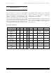
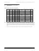
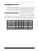
Data Register CE2- CE1- A0 Offset Data Bus
Word Data Register 0 0 X 0,8,9 D15-D0
Even Data Register 1 0 0 0,8 D7-D0
Odd Data Register 1 0 1 9 D7-D0
Odd Data Register 0 1 X 8,9 D15-D8
Error / Feature Register 1 0 1 1, Dh D7-D0
Error / Feature Register 0 1 X 1 D15-D8
Error / Feature Register 0 0 X Dh D15-D8